
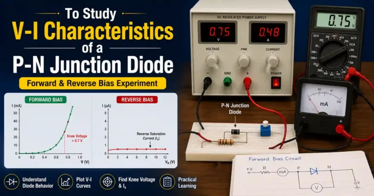
Welcome to one of the most foundational experiments in engineering physics! Today, we are exploring the V-I characteristics of PN junction diodes.
Contents
Toggle📖 Introduction:
The V-I characteristics of PN junction diode experiment are one of the most fundamental experiments in engineering physics and basic electronics. It helps students understand how a semiconductor diode behaves under forward-bias and reverse-bias conditions by studying the relationship between the applied voltage and the current flowing through the diode.
In this experiment, students observe that the diode allows a large current to flow after a certain forward voltage (called the knee or cut-in voltage), while only a very small leakage current flows in reverse bias until breakdown occurs. Understanding these characteristics is essential for analyzing electronic circuits and semiconductor devices.
If you are new to semiconductor physics, you may also like to read our detailed articles on the formation of P-N junctions, energy band theory, intrinsic and extrinsic semiconductors, and semiconductor diodes, which provide the theoretical background required to understand this experiment thoroughly.
🚀 Aim of the experiment:
To study the voltage-current (V-I) characteristics of PN junction diode under forward bias and reverse bias conditions and determine the knee voltage and reverse saturation current.
🎯 Importance of this Experiment:
This experiment is much more than simply plotting a graph. It helps students visualize the actual behavior of semiconductor devices and bridges the gap between theoretical concepts and practical applications.
Through this practical, students learn the following:
- Understanding of semiconductor diode operation
- Difference between forward and reverse bias
- Concept of cut-in (threshold) voltage
- Reverse saturation current
- Dynamic resistance of diode
- Practical use of semiconductor devices
- Characteristics of non-linear electronic components
🌍 Engineering Physics Importance:
The experiment is important because it introduces students to one of the most widely used semiconductor devices in modern electronics. The principles learned here serve as the basis for understanding:
- Rectifier Circuits
- Voltage Regulators
- Signal Clipping and Clamping Circuits
- LED and Laser Diodes
- Solar Cells
- Photodiodes
- Transistors
- Digital Electronics
💡 Deep Dive: Key Concepts to Remember:
To truly grasp this V-I characteristics experiment, you need to understand what is happening inside the crystal lattice. When the P-type and N-type semiconductors merge, they form a depletion region.
In forward bias, the applied voltage counteracts this internal barrier. Once you cross the knee voltage (around 0.7 V for silicon), the barrier drops, and current surges.
In reverse bias, the applied voltage widens the barrier, blocking current flow except for a tiny minority carrier leakage current.
📝 Experiment Summary:
Before performing any laboratory experiment, it is helpful to understand its objective and expected outcome. This experiment provides a practical demonstration of how the current through a P-N junction diode changes with the applied voltage in both forward and reverse bias conditions.
| Parameter | Description |
|---|---|
Experiment Name |
To Study V-I Characteristics of P-N Junction Diode |
Objective |
To plot the forward and reverse bias V-I characteristics of a P-N junction diode |
Apparatus Required |
P-N Junction Diode, Regulated DC Supply, Milliammeter, Microammeter, Voltmeter, Rheostat, Connecting Wires |
Forward Bias connection |
Positive to P-type, Negative to N-type |
Reverse bias connection |
Positive to N-type, Negative to P-type |
Observation |
Measure current corresponding to different applied voltages |
Graph |
Voltage vs Current |
Result |
Determine cut-in voltage and study diode behavior in forward and reverse bias |
📋Observation Table:

📄 Lab Manual PDF:
To help you follow along in the lab, here is the official, high-quality lab manual PDF. You can view, download, or print it for your practical sessions.
📄Modified Lab Manual PDF:
🎥 Recommended Tutorial:
🎓 Exam-Oriented Questions & Answers:
## What is a P-N junction diode?
**Answer:**
A P-N junction diode is a semiconductor device formed by joining P-type and N-type semiconductor materials. It allows current to flow easily in one direction (forward bias) while offering high resistance in the opposite direction (reverse bias).
## What is the knee voltage of a silicon diode?
**Answer:**
The knee (cut-in) voltage of a silicon diode is approximately 0.7 V. Beyond this voltage, the diode conducts current rapidly in the forward-bias region.
## Why is reverse saturation current very small?
**Answer:**
Reverse saturation current is produced by minority charge carriers. Since their concentration is very low, only a small current flows in reverse bias before breakdown occurs.
## What is Cut-in Voltage?
**Answer:**
The minimum forward voltage at which the diode begins to conduct appreciable current is called the cut-in voltage.
Typical values:
- Silicon Diode ≈ 0.7 V
- Germanium Diode ≈ 0.3 V
## Why is Reverse Current Small?
**Answer:**
Under reverse bias, only minority charge carriers contribute to current flow. Hence, the reverse current remains extremely small until breakdown occurs.
## Why is the Graph Non-linear?
**Answer:**
Unlike an ordinary resistor that follows Ohm’s Law, a P-N junction diode is a non-linear device. Therefore, current does not increase in proportion to voltage.
## What is the aim of the V-I characteristics experiment?
**Answer:**
The aim is to study the relationship between voltage and current in a P-N junction diode under forward and reverse bias conditions and determine its cut-in voltage from the V-I characteristics.
## Why is a diode called a non-linear device?
**Answer:**
A diode is called non-linear because its current is not directly proportional to the applied voltage. Its V-I graph is not a straight line.
## What is the significance of the V-I characteristics curve?
**Answer:**
The V-I curve helps determine the diode’s conducting behavior, threshold voltage, dynamic resistance, and suitability for electronic circuit applications.
## Why is reverse current called saturation current?
**Answer:**
Because it depends on the number of minority carriers, which is fixed at a given temperature. Increasing reverse voltage doesn’t increase this current until breakdown occurs.
## What is dynamic resistance of a diode?
**Answer:**
It is the ratio of a small change in voltage to the resulting change in current, calculated from the slope of the forward characteristic curve near the operating point.
## Why does reverse current increase suddenly at breakdown voltage?
**Answer:**
At breakdown, the electric field becomes strong enough to trigger avalanche or Zener effects, generating a large number of charge carriers and causing a sharp current rise.
## Is the PN junction diode a linear or non-linear device?
**Answer:**
It is non-linear, since current does not increase proportionally with voltage—this is clearly visible from the curved, exponential shape of the forward characteristic.
## What is the difference between static and dynamic resistance?
**Answer:**
Static resistance is simply V/I at a particular point, while dynamic resistance is the slope ΔV/ΔI, representing how resistance changes locally on the curve.
## Why do we use a milliammeter in forward bias but a microammeter in reverse bias?
**Answer:**
Because forward current is in the milliampere range while reverse current is thousands of times smaller, in the microampere range—using the wrong meter would give an unreadable or inaccurate result.
## What happens to the depletion region width under forward and reverse bias?
**Answer:**
It narrows under forward bias, allowing carriers to cross easily, and widens under reverse bias, further restricting carrier movement.
🎤 Viva Questions and Answers:
Q1. What is a semiconductor diode?
Answer: A semiconductor device formed by joining P-type and N-type materials.
Q2. What is forward bias?
Answer: Connecting the P-side to the positive terminal and the N-side to the negative terminal.
Q3. What is reverse bias?
Answer: Connecting the P-side to the negative terminal and the N-side to the positive terminal.
Q4. What is knee voltage?
Answer: The minimum forward voltage required for significant conduction.
Q5. What is reverse saturation current?
Answer: The small reverse current due to minority carriers.
Q6. Which carriers conduct current in forward bias?
Answer: Majority charge carriers.
Q7. Which carriers conduct current in reverse bias?
Answer: Minority charge carriers.
Q8. Why is a milliammeter used in forward bias?
Answer: Because forward current is relatively large.
Q9. Why is a microammeter used in reverse bias?
Answer: Because reverse current is very small.
Q10. Name two applications of P-N junction diode.
Answer: Rectifiers and voltage protection circuits.
Q11: What is ideal diode resistance in forward and reverse bias?
Ans: An ideal diode offers zero resistance in forward bias (acting as a closed switch) and infinite resistance in reverse bias (acting as an open switch).
Q12: What causes Zener breakdown?
Ans: Zener breakdown occurs in heavily doped diodes under high reverse voltage. The intense electric field across the narrow depletion layer directly ruptures covalent bonds, generating a massive surge of current.
❓Frequently Asked Questions (FAQs):
# What is the objective of the V-I characteristics of a P-N junction diode experiment?
The objective is to study the current-voltage relationship of a P-N junction diode under forward and reverse bias conditions and determine its cut-in voltage.
# Why is the V-I characteristics experiment important?
It helps students understand the practical behavior of semiconductor diodes, which are the building blocks of almost every electronic device.
# What is the difference between forward bias and reverse bias?
In forward bias, the diode conducts current after the cut-in voltage. In reverse bias, only a very small leakage current flows until breakdown.
# Why is the diode called a one-way conductor?
Because it allows current to flow easily in one direction (forward bias) while blocking current in the opposite direction (reverse bias).
# Why is the forward characteristic curve non-linear?
Because diode current follows an exponential relationship with voltage (as per the Shockley diode equation), not a linear one, so equal increases in voltage do not produce equal increases in current.
# What is the typical cut-in voltage for silicon and germanium diodes?
Silicon diodes typically show a cut-in voltage of about 0.6 to 0.7V, while germanium diodes show a lower cut-in voltage of around 0.2 to 0.3V.
# Why does reverse current remain almost constant with increasing reverse voltage?
Because it is limited by the number of available minority charge carriers rather than by the applied voltage, it stays nearly constant until the breakdown voltage is reached.
# Why does temperature affect the V-I characteristics?
Temperature gives charge carriers more thermal energy. An increase in temperature lowers the knee voltage in forward bias and increases the reverse saturation leakage current.
# Can we use an ordinary multimeter to check if a diode works?
Yes. Using the "Diode Test" mode, a multimeter applies a small voltage. If it reads around $0.7\text{ V}$ in one direction and "OL" (Overload/Open Loop) in reverse, the diode is functioning correctly.
# What is the difference between avalanche and Zener breakdown?
Zener breakdown occurs in heavily doped diodes due to strong electric fields pulling electrons out of bonds. Avalanche breakdown happens in lightly doped diodes where high-velocity minority carriers collide with atoms, creating a chain reaction.
🔗 Related Experiments:
Ready to explore more in the physics lab? Check out these step-by-step experiment guides:
- Determination of Energy Band Gap of a Semiconductor
- Study of Zener Diode Characteristics
- Half-Wave Rectifier Experiment
- Full Wave Rectifier Experiment
- Bridge Rectifier Experiment
- Study of LED Characteristics
- Photodiode Characteristics
- Solar Cell Characteristics
- Verification of Ohm’s Law