
Want to understand why a diode suddenly starts conducting after a small voltage? Read the complete article below and follow the I-V characteristics from the microscopic movement of charge carriers to the mathematical diode equation.

Contents
ToggleIntroduction
A diode looks like a very simple electronic component: it has only two terminals, an anode and a cathode. Yet its electrical behavior is far more interesting than that of an ordinary resistor.
The relationship between the voltage applied across the diode and the current flowing through it is called the I–V characteristics of a p–n junction diode.
The I-V characteristics of the diode are crucial, as it works as a rectifier, which enables current flow in one direction (forward bias) while preventing it in the opposite direction (reverse bias). This behavior of the junction diode is illustrated by the I-V characteristics curve, which is described by the Shockley diode equation: $$I=I_S\left(e^{\frac{qv}{\eta kT}}-1\right) $$
where Is represents the reverse saturation current. A practical application of this is in smartphone chargers, which convert alternating current (AC) to direct current (DC) for safe charging of devices.
The p-n junction diode plays a vital role in converting AC to DC due to its unique I-V characteristics that describe current flow under varying voltage conditions, effectively indicating whether the diode allows current flow or blocks it depending on the voltage applied.
By the end of this article, you will clearly understand:
- How current varies with voltage in a diode
- Why a diode behaves differently in forward and reverse bias
- The mathematical equation governing this behavior
- Real-world applications of these characteristics
If you have already studied the [formation of a p–n junction], the [depletion region], and the [built-in potential], this article will connect those concepts directly to the experimentally observed diode characteristic.
I-V Characteristics of a p–n Junction Diode
The I-V characteristics of a p–n junction diode describe the mathematical and graphical relationship between the voltage across the diode’s terminals and the electric current flowing through it, which describes how current (I) varies with applied voltage (V). Unlike a standard carbon resistor, which loyally follows Ohm’s law with a linear response, a diode is fundamentally non-linear.
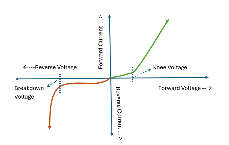
These characteristics have two parts: one for forward bias and one for reverse bias. As shown in the following figure.
I-V Characteristics in Forward Bias
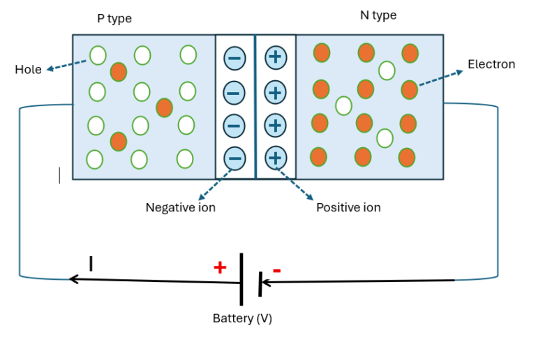
When the p-side is connected to the positive terminal and the n-side to the negative terminal of the external supply voltage (battery), as connected in the above figure, the diode is in the forward-bias condition. In this case:
- Barrier potential decreases
- Charge carriers cross the junction easily
- Current increases rapidly
Imagine it like opening a floodgate; once the barrier is reduced, the current flows freely.
The Shockley equation $$I\propto e^{\frac{qV}{kT}} $$ explains why the forward current increases exponentially rather than linearly.
Let’s understand the junction diode’s behavior under externally applied forward voltages.
Low-Voltage Region
When a small forward voltage is applied:
- The potential barrier reduces slightly.
- Only a small current flows.
- Current increases slowly at first.
This region is sometimes called the cut-in or knee region.
Cut-in (Threshold) Voltage Region
The voltage at which the forward current begins increasing rapidly is commonly called the knee voltage, cut-in voltage, or threshold voltage. It is nearly 0.7 V for a silicon diode and nearly 0.3 V for a germanium diode. It depends on temperature, device construction, and other factors.
Rapid-Conduction Region
Beyond the knee region,
- The barrier becomes very small.
- The majority of carriers cross the junction easily.
- Current rises rapidly.
Hence, a relatively small increase in voltage can produce a large increase in current.
This is the region responsible for the familiar steep portion of the diode I–V curve.
I–V Characteristics in Reverse Bias
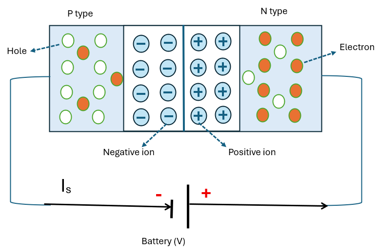
When the p-side is connected to the negative terminal and the n-side to the positive terminal of the battery, as connected in the above circuit diagram, the diode is in the reverse-bias condition.
Let’s examine the behavior of the junction diode under externally applied reverse-bias voltages.
Behaviour Under Reverse Bias
When reverse voltage is applied, the following changes appear:
- Potential barrier increases.
- Depletion region widens.
- Majority charge carriers move away from the junction.
- Only minority carriers contribute
- Current flow is extremely small
👉 This works like a closed valve, only with tiny leakage.
Reverse Saturation Current
When reverse bias voltage is applied, the current increases slightly, and then it becomes nearly constant. Until the breakdown region is reached, this current, which has a very small magnitude, is almost unaffected by the reverse voltage that is applied. It is called the reverse saturation current.
However, it is temperature-dependent, rising sharply as the temperature rises because of large charge carrier generation.
Breakdown Region
When a high reverse voltage is applied, the diode’s behavior drastically changes; the current, which was previously very low, suddenly increases. This abrupt increase in current is due to the breakdown process within the junction. The reverse applied voltage at which the current increases abruptly is called the breakdown voltage.
This breakdown can occur in one of two ways:
- Zener breakdown:
When a p–n junction is heavily doped, its depletion region becomes very narrow. Under a sufficiently large reverse-bias voltage, the electric field across this narrow region becomes extremely strong. This strong field can cause electrons to tunnel through the junction, resulting in a sudden increase in reverse current. This phenomenon is known as Zener breakdown.
Zener breakdown generally occurs at relatively low reverse voltages in heavily doped junctions.
- An avalanche breakdown:
Avalanche breakdown occurs when a reverse-biased p–n junction is subjected to a sufficiently high electric field. The charge carriers moving through the depletion region gain enough kinetic energy to collide with atoms and generate additional electron–hole pairs.
These newly generated carriers are accelerated by the electric field and can create still more electron–hole pairs. This chain reaction produces carrier multiplication, causing the reverse current to rise sharply. This process is called avalanche breakdown.
The breakdown voltage and the relative contribution of Zener and avalanche mechanisms depend on factors such as doping concentration, depletion-region width, junction structure, temperature, and semiconductor material.
Factors that Affect I-V Characteristics
- Temperature
- The reverse saturation current increases strongly with temperature in reverse bias.
- But in forward bias, the cut-in voltage decreases slightly with temperature.
- Semiconductor Material
- I-V characteristics are also affected by the material used to form the junction diode, as silicon has a higher threshold voltage than germanium.
- Doping Level
- The doping concentration affects breakdown voltage and leakage current.
Comparison Between Forward and Reverse Bias Characteristics
| Property | In Forward Bias | In Reverse Bias |
|---|---|---|
Barrier potential |
Decreases |
Increases |
Depletion width |
Narrows |
Widens |
Current magnitude |
Large |
Very small |
Carrier type |
Majority |
Minority |
Curve nature |
Exponential rise |
Nearly constant |
Interactive Diode Junction & I-V Response
State: Equilibrium (No Current Flow)
Important Features of the I–V Curve
The major features that students should identify on an I–V graph are
1. Origin: The curve passes through or very near the origin under the idealized model because the net diode current is zero when the applied voltage is zero.
2. Forward-Bias Region: The current becomes positive and eventually increases very rapidly.
3. Knee Voltage: This marks the region where substantial forward conduction becomes evident on the practical characteristic.
4. Reverse-Bias Region: Only a small reverse current flows before breakdown.
5. Breakdown Voltage: At sufficiently high reverse voltage, the current increases sharply.
These features form the basis of most examination questions involving the diode I–V characteristic.
Static and Dynamic Resistance of a Diode
Because the diode has a nonlinear I–V relationship, two different resistance concepts are useful.
Static or DC Resistance: The static resistance at a particular operating point is $$R_{dc}=\frac{V_D}{I_D}$$
It represents the ratio of voltage to current at that particular point on the I–V curve.
Dynamic or AC Resistance: The dynamic resistance is the slope-based resistance: $$r_d=\frac{dV}{dI}$$
Starting from the diode equation under forward bias,
$$I\approx I_S e^{V/ηV_T}$$
Taking the derivative,
$$dI = I_S e^{V/ηV_T}\left( 1/ηV_T \right) dV$$
$$\frac{dV}{dI} = \frac{\eta V_T}{I}$$
Thus,
$$r_d=\frac{ηV_T}{I}$$
This result has a useful physical interpretation.
As the forward current increases, the dynamic resistance decreases.
That is why the I–V curve becomes steeper at larger forward currents.
Real-World Engineering Applications
The I–V characteristics of a p–n junction diode are used to design a special-purpose diode for various applications in different electric circuits, such as
- Rectifiers → for AC to DC conversion
- Clipping circuits → for waveform shaping
- Voltage regulators → using Zener breakdown
- Signal detection → in radio receivers
- Switching circuits → in digital electronics
Conclusion
The I–V characteristics of a p–n junction diode reveal the true behavior of this most important electronic device.
The main takeaways are the following:
- In forward bias, current increases exponentially
- While in reverse bias, the current is extremely small and constant
- Diode behavior can be described by the Shockley equation
- Temperature affects its performance significantly.
👉 In modern engineering, understanding this curve is like understanding the heartbeat of electronics.
Solved Numerical Problems
Numerical Problem 1: Forward Current Using the Diode Equation
Question: A silicon p–n junction diode has a reverse saturation current of 2 nA. It is operated at 300 K with an ideality factor (η=1.8). Calculate the diode current when the applied forward voltage is 0.62 V.
Solution
Given:
$$I_S=2\times 10^{-9}\text{ A}$$
$$η=1.8$$
$$V=0.62\text{ V}$$
$$T=300\text{ K}$$
At 300 K,
$$V_T\approx25.85\text{ mV}$$
or
$$V_T=0.02585\text{ V}$$
Find: (I)
Using
$$I=I_S\left(e^{V/ηV_T}-1\right)$$
Substituting,
$$I=2\times10^{-9}
\left[e^{0.62/(1.8\times0.02585)}-1\right]$$
The exponent is approximately
$$\frac{0.62}{1.8\times0.02585}\approx13.32$$
Therefore,
$$I\approx1.22\times 10^{-3}\text{ A}$$
Hence,
$${I\approx1.22\text{ mA}}$$
Answer: The forward diode current is approximately 1.22 mA.
Numerical Problem 2: Reverse Current
Question: A diode has a reverse saturation current of 3.5 nA. Determine the diode current when a reverse voltage of 4 V is applied at 300 K, assuming the diode has not reached breakdown.
Solution:
Given: $$I_S=3.5\times 10^{-9}\text{ A}$$
$$V=-4\text{ V} $$
For reverse bias,
$$I=I_S\left(e^{V/ηV_T}-1\right)$$
Since the exponent is strongly negative,
$$e^{V/ηV_T}\approx0$$
Therefore,
$$I\approx-I_S$$
Thus,
$$I\approx-3.5\times 10^{-9}\text{ A}$$
Hence,
$${I\approx-3.5\text{ nA}}$$
Answer: The reverse current is approximately 3.5 nA in the reverse direction.
Numerical Problem 3: Dynamic Resistance
Question: A diode operates at a forward current of 8 mA at 300 K. If the ideality factor is η=1.5, calculate its dynamic resistance.
Solution
Given: $$
I=8\times 10^{-3}\text{ A}$$
$$η=1.5$$
$$V_T=25.85\times 10^{-3}\text{ V}$$
Find: (rd)
Using
$$r_d=\frac{ηV_T}{I}$$
we obtain
$$r_d=\frac{1.5(25.85\times10^{-3})}8\times10^{-3}$$
Therefore,
$$r_d\approx4.85\Omega$$
Hence,
$${r_d\approx4.85\Omega}$$
Answer: The dynamic resistance of the diode is approximately 4.85 Ω.
Numerical Problem 4: Diode Power
Question: A forward-biased diode has a voltage drop of 0.66 V and carries a current of 24 mA. Calculate the power dissipated by the diode.
Solution:
Given: $$V=0.66\text{ V}$$
$$I=24\times 10^{-3}\text{ A}$$
Find: (P)
Using
$$P=VI$$
we get
$$P=(0.66)(24\times10^{-3})$$
$$P=15.84\times 10^{-3}\text{ W}$$
Therefore,
$${P=15.84\text{ mW}} $$
Answer: The diode dissipates approximately 15.84 mW.
People Also Ask Questions
# What are the I–V characteristics of a p–n junction diode?
The I–V characteristics of a p–n junction diode describe how diode current changes with applied voltage. Under forward bias, current stays relatively small initially, then rises rapidly after the knee. Under reverse bias, only a small reverse saturation current flows until the reverse voltage reaches breakdown, where current increases sharply.
# What is the knee voltage of a p–n junction diode?
The knee voltage is the approximate forward voltage at which a practical diode current begins to increase rapidly. It is commonly taken as about 0.7 V for silicon and about 0.3 V for germanium in basic circuit analysis. The actual value varies with current, temperature, and device construction.
# What happens to a diode under forward bias?
Under forward bias, the p-side is connected to the positive terminal and the n-side to the negative terminal. The applied voltage reduces the junction barrier and narrows the depletion region. As a result, majority carriers cross the junction more easily, causing the forward current to increase rapidly with applied voltage.
# What happens to a diode under reverse bias?
Under reverse bias, the p-side is connected to the negative terminal and the n-side to the positive terminal. The applied voltage increases the junction barrier and widens the depletion region. Majority-carrier flow is strongly suppressed, leaving only a small reverse current mainly associated with minority carriers.
# What is reverse saturation current?
Reverse saturation current is the small current that flows through a reverse-biased p–n junction before breakdown. It is represented by IS in the Shockley diode equation. Its magnitude depends on the semiconductor material, junction properties, and temperature, and it generally increases significantly as temperature rises.
# What is breakdown voltage in a diode?
Breakdown voltage is the reverse-bias voltage at which the reverse current of a p–n junction increases sharply. Breakdown can occur through mechanisms such as Zener tunnelling or avalanche carrier multiplication, depending on junction properties. An ordinary diode may be damaged if its rated reverse voltage or power limits are exceeded.
# What is the difference between static and dynamic resistance of a diode?
Static resistance is the ratio of diode voltage to current at an operating point (R=V/I). Dynamic resistance is the local slope of the I–V curve (rd=dV/dI). For the exponential diode model, dynamic resistance is approximately (nVT/I), so it decreases as forward current increases.
# Why is a diode called a nonlinear device?
A diode is called nonlinear because its current is not directly proportional to its voltage. Unlike an ideal resistor, its I–V relationship is approximately exponential in forward conduction and nearly constant at a small reverse saturation current before breakdown.
Important Questions
- Explain the I–V characteristics of a p–n junction diode with a neat graph.
- Derive the Shockley equation for a p–n junction diode.
- Derive the expression for the dynamic resistance of a diode.
- Explain the forward and reverse characteristics of a p–n junction diode.
- Explain the physical mechanisms responsible for diode breakdown.
- Derive the diode current equation using minority-carrier diffusion.
- Explain the effect of applied voltage on the potential barrier and depletion region.
FAQs
1. What are I–V characteristics of a diode?
It is a curve that describes how current varies with applied voltage.
2. Why is diode current exponential?
Diode current is exponential because of carrier diffusion and barrier reduction.
3. What is cut-in voltage?
Cut-in voltage (also called threshold voltage) is the minimum forward voltage required for significant conduction.
4. Why is reverse current small?
Reverse current in a diode is very small because it is mainly due to minority charge carriers.
5. What happens during breakdown?
During breakdown, a sudden increase in reverse current occurs when the applied voltage exceeds a critical value called the breakdown voltage.
The explanation of the diode’s I–V characteristics is clear and well structured. I especially like how the article connects the forward and reverse bias regions with practical applications, making the concept easier to understand for students.
Thank you