
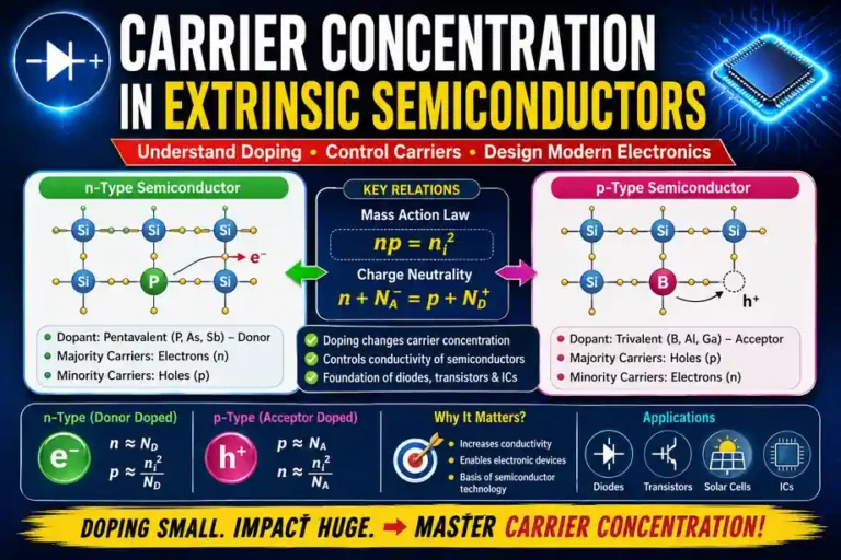
A tiny amount of impurity can completely change the electrical behavior of a semiconductor. But how can adding only a few impurity atoms produce such a large change in conductivity? The answer lies in the number of electrons and holes available for conduction, known as carrier concentration.
The carrier concentration in extrinsic semiconductors can be precisely controlled through doping, enabling the design of materials for specific electronic applications. Let us now explore how carrier concentration is determined in n-type and p-type semiconductors and why it is so important in semiconductor devices.
Contents
Toggle🚀 Introduction: Extrinsic Carrier Concentration
Carrier concentration in extrinsic semiconductors refers to the number of free electrons or holes in a semiconductor after adding impurity atoms through doping. Unlike intrinsic semiconductors, where carriers are generated naturally, doping introduces extra energy levels that increase electrical conductivity and make the material useful for electronic devices.
When donor or acceptor impurities are added, the semiconductor becomes n-type or p-type, increasing majority charge carriers. The carrier concentration mainly depends on doping level and temperature, and it plays an important role in understanding semiconductor conductivity and device behavior.
Now, to understand extrinsic carrier concentration in detail, let us study it separately for n-type and p-type semiconductors, where the roles of majority and minority charge carriers are different.
By the end of this article, you’ll be able to derive the majority carrier concentration formula from first principles and solve numerical problems.
🧠 Core Concept: What Decides Extrinsic Carrier Concentration?
An extrinsic semiconductor is simply a pure (intrinsic) semiconductor crystal that has been deliberately “impurified”—a process called “doping”—with a controlled number of foreign atoms. Depending on which impurity you add, you get two types of extrinsic semiconductors:
1. n-type Semiconductor (Donor Doping):
When a small amount of a pentavalent (Group V) impurity, such as phosphorus, arsenic, or antimony, is added to a pure semiconductor like silicon, it transforms the material into an n-type semiconductor.
The impurity has five valence electrons. Four of them form covalent bonds with the neighboring silicon atoms, while the fifth electron remains only weakly attached to the impurity atom. It therefore needs only a small amount of thermal energy, typically about 0.01–0.05 eV, to become free and move into the conduction band.
Since the impurity contributes an extra electron to the semiconductor, it is called a donor impurity. As a result, free electrons become the majority carriers in the n-type semiconductor.
2. p-type Semiconductor (Acceptor Doping):
When a small amount of a trivalent (Group III) impurity, such as boron, gallium, or indium, is added to a pure semiconductor, it produces a p-type semiconductor.
Unlike silicon, which has four valence electrons, the trivalent impurity has only three. As a result, it can form only three complete covalent bonds with its neighboring silicon atoms, leaving one bond incomplete. This missing electron creates a hole, which can move through the crystal and contribute to electrical conduction.
Since the impurity tends to accept an electron from a neighboring covalent bond to complete the missing bond, it is called an acceptor impurity. Consequently, holes become the majority carriers, while electrons remain the minority carriers.
This brings us to an important relationship that connects the concentrations of these two types of carriers. Whether the semiconductor is n-type or p-type, the law of mass action provides a simple relationship between electron concentration and hole concentration.
Let’s see how to derive the majority carrier concentration in n-type and p-type semiconductors.
⚡ Extrinsic Carrier Concentration & Fermi Level Simulator
Adjust temperature and doping levels to observe carrier distribution and Fermi level ($E_F$) shift.
🧮 Derivation of Extrinsic Carrier Concentration:
Let’s derive the exact expressions for carrier concentration for both N-type and P-type semiconductors from first principles.
Majority Carrier Concentration in n-type Semiconductor:
Let ND be the concentration of donor atoms in an n-type semiconductor. At 0 K, donor atoms are not ionized and lie at the donor energy level ED, which is very close to the bottom of the conduction band energy level EC.
When the temperature increases above 0 K, donor atoms get ionized and free electrons appear in the conduction band.
Hence, the electron concentration in the conduction band is given by:
$$n = N_D^+ =N_D-N_D^0$$
where,
ND+= number of ionized donor atoms and
ND0= number of un-ionized donor atoms
The concentration of ionized donors is:
$$N_D^+ =N_D\left[ 1-f\left( E_D \right) \right] ———-(1)$$
And as per the Fermi–Dirac distribution function:
$$f\left( E_D \right) =\frac{1}{1+ exp\left( \frac{E_D-E_F}{kT} \right)}———–(2)$$
In an n-type semiconductor, the Fermi level lies between the donor level and the conduction band bottom level. Hence, it is negative.
Therefore: $$1-f\left( E_D \right) =exp\left( \frac{E_D-E_F}{kT} \right)—————(3)$$
Substituting this in eq. (1), we get the following:
$$n=N_D^+ =N_D exp\left( \frac{E_D-E_F}{kT} \right)————–(4)$$
But the electron concentration in the conduction band is also given by:
$$n= N_C exp\left[ -\left( \frac{E_C-E_F}{kT} \right) \right]————-(5)$$
Comparing the above equations (4) and (5), we get:
$$N_C exp\left[ -\left( \frac{E_C-E_F}{kT} \right) \right]=N_D exp\left( \frac{E_D-E_F}{kT} \right) $$
$$=>exp\left[ \left( \frac{2E_F-E_D-E_C}{kT} \right) \right]=\frac{N_D}{N_C}$$
Taking the logarithm and solving, the Fermi level is:
$$E_F=\frac{E_D+E_C}{2}+\frac{kT}{2}log_{e}\left( \frac{N_D}{N_C} \right)———-(6)$$
At T = 0 K: $$E_F=\frac{E_D+E_C}{2}$$
Thus, the Fermi level lies midway between the donor level and the bottom of the conduction band.
Substituting the value of EF from equation (6) in equation (5), we get:
$$n= N_C exp\left[ -\left( \frac{E_C-\left( \frac{E_D+E_C}{2}+\frac{kT}{2}log_{e}\left( \frac{N_D}{N_C} \right) \right)}{kT} \right) \right]$$
$$n= N_Cexp\left( \frac{E_D-E_C}{2kT} \right)exp\left[ \frac{1}{2}log_{e}\left( \frac{N_D}{N_C} \right) \right]$$
$$n= \left(N_DN_C\right)^{1/2}exp\left( \frac{E_D-E_C}{2kT}\right) $$
The final expression for electron concentration is:
$$n= \left(2N_D\right)^{1/2}\left( \frac{2\pi m_e^*kT}{h^2} \right)^{3/4}exp\left( \frac{E_D-E_C}{2kT}\right) $$
Majority Carrier Concentration in a p-type Semiconductor:
Let NA be the concentration of acceptor atoms in a p-type semiconductor. At 0 K, acceptor atoms are not ionized and lie at the acceptor energy level, which is very close to the valence band energy level.
When the temperature increases, the acceptor starts ionizing, and correspondingly, an electron from the valence band jumps to the acceptor level; therefore, a hole is created in the valence band.
Hence, the hole concentration is given by:
$$p = N_A^-$$
where,
NA–= number of ionized acceptor atoms
The concentration of ionized acceptor is:
$$N_A^-=N_Af\left( E_A \right) ———-(7)$$
And as per the Fermi–Dirac distribution function:
$$f\left( E_A \right) =\frac{1}{1+ exp\left( \frac{E_A-E_F}{kT} \right)}———–(8)$$
Since the acceptor level lies above the Fermi level, (EA – EF) is positive. Therefore:
$$p=N_A exp\left( \frac{E_F-E_A}{kT} \right)————–(9)$$
But hole concentration in the valence band is also given by:
$$p= N_V exp\left[ -\left( \frac{E_F-E_V}{kT} \right) \right]————-(10)$$
Comparing the above equations (9) and (10), we get:
$$N_V exp\left[ -\left( \frac{E_F-E_V}{kT} \right) \right]=N_A exp\left( \frac{E_F-E_A}{kT} \right)$$
$$=>exp\left[ \left( \frac{2E_F-E_A-E_V}{kT} \right) \right]=\frac{N_V}{N_A}$$
Taking the logarithm and solving, the Fermi level is:
$$E_F=\frac{E_A+E_V}{2}+\frac{kT}{2}log_{e}\left( \frac{N_V}{N_A} \right)———-(11)$$
At T = 0 K:
$$E_F=\frac{E_A+E_V}{2}$$
Thus, the Fermi level lies midway between the acceptor level and the top of the valence band.
Substituting the value of EF from equation (11) in equation (9), we get:
$$p= N_A exp\left( \frac{\left( \frac{E_A+E_V}{2}+\frac{kT}{2}log_{e}\left( \frac{N_V}{N_A} \right)-E_A \right)}{kT} \right)$$
$$p= N_Aexp\left( \frac{E_V-E_A}{2kT} \right)exp\left[ \frac{1}{2}log_{e}\left( \frac{N_V}{N_A} \right) \right]$$
$$p= \left(N_AN_V\right)^{1/2}exp\left( \frac{E_V-E_A}{2kT}\right)$$
The final expression for hole concentration is:
$$p= \left(2N_A\right)^{1/2}\left( \frac{2\pi m_h^*kT}{h^2} \right)^{3/4}exp\left( \frac{E_V-E_A}{2kT}\right)$$
⚖️ Intrinsic vs Extrinsic Carrier Concentration:
| Property | Intrinsic Semiconductor | Extrinsic Semiconductor |
|---|---|---|
Source of carriers |
Thermal breaking of covalent bonds only |
Doping (donor/acceptor atoms) + thermal generation |
Electron : Hole ratio |
Always equal, n = p = nᵢ |
Highly unequal—majority vs minority carriers |
Conductivity |
Very low, strongly temperature-dependent |
Much higher, controllable by doping level |
Concentration formula |
nᵢ = √(Nc.Nv) exp(-Eg/2kT) |
n ≈ N_D (n-type) |
Practical use |
Reference material, rarely used alone |
Backbone of diodes, transistors, ICs, solar cells |
✅ Advantages and ⚠️ Limitations of the Extrinsic Carrier Concentration:
Advantages: The formulas are algebraically simple in the saturation region; they let engineers predict device behaviour before fabrication, and the law of mass action provides a universal check that works regardless of doping type or level.
Limitations: The simple approximation (n ≈ ND) breaks down at very low temperatures (freeze-out) and very high temperatures (intrinsic region); full ionization is assumed, which isn’t perfectly true near absolute zero, and the model ignores band-gap narrowing that occurs at extremely heavy doping levels (above roughly 10-19 cm-3).
⚙️ Real-World Applications of Extrinsic Carrier Concentration:
- PN junction diodes: The built-in potential and depletion width both depend directly on ND and NA through the carrier concentration equations derived above.
- Bipolar transistors: Current gain is engineered by carefully choosing different doping (and hence carrier) concentrations in the emitter, base, and collector regions.
- Solar cells: Minority carrier concentration (p = ni2/ND) directly controls how efficiently a solar cell can collect light-generated carriers before they recombine.
- Thermistors and temperature sensors: The predictable freeze-out-to-intrinsic transition curve you explored in the simulator is exploited to build precision temperature sensors.
- Integrated circuit fabrication: Ion-implantation doses in modern chip manufacturing are calculated directly from the target carrier concentration using these very equations.
🔎 Quick Answer Section: Extrinsic Carrier Concentration
## What is carrier concentration in extrinsic semiconductors?
Carrier concentration is the number of free charge carriers present per unit volume of an extrinsic semiconductor. Depending on the doping, either electrons or holes become majority carriers. In n-type material, electrons dominate, while in p-type material, holes dominate.
## What is the formula for carrier concentration in an n-type semiconductor?
For a strongly doped n-type semiconductor with complete donor ionization, the majority electron concentration is approximately equal to the donor concentration:
$$n\approx N_D$$
The minority hole concentration is obtained from the mass action law:
$$p=\frac{n_i^2}{N_D}$$
## What is the carrier concentration of a p-type semiconductor?
In a strongly doped p-type semiconductor, holes are the majority carriers, and their concentration is approximately equal to the acceptor concentration:
$$p\approx N_A$$
The minority electron concentration is:
$$n\approx\frac{n_i^2}{N_A}$$
## What are majority and minority carriers?
Majority carriers are the charge carriers present in greater concentration, while minority carriers are present in smaller concentration. Electrons are majority carriers in n-type semiconductors, whereas holes are majority carriers in p-type semiconductors.
## Why are electrons majority carriers in an n-type semiconductor?
An n-type semiconductor is doped with pentavalent donor atoms. Each donor atom contributes an additional electron that can become a conduction electron. Consequently, electrons become much more numerous than holes.
## Why does carrier concentration increase after doping?
Doping introduces donor or acceptor impurity atoms into the semiconductor. Donors provide additional electrons, while acceptors increase the number of holes. Therefore, the concentration of electrically active carriers increases.
## What is a compensated semiconductor?
A compensated semiconductor contains both donor and acceptor impurities simultaneously. Its net carrier concentration is found from the exact charge-neutrality equation, and its type (n or p) depends on whichever impurity concentration is larger.
## What is the unit of carrier concentration?
Carrier concentration is measured in the number of carriers per unit volume, typically expressed as cm⁻³ in most textbooks or m⁻³ in SI-consistent calculations.
## Why does carrier concentration become constant in the saturation region?
In the saturation (extrinsic) temperature region, ambient thermal energy is high enough to ionize all donor or acceptor dopant atoms, yet low enough that intrinsic band-to-band generation is negligible. Consequently, carrier concentration remains fixed at the dopant density (n ≈ ND).
## What happens to extrinsic semiconductors at very high temperatures?
At high temperatures, thermal energy generates electron-hole pairs across the fundamental bandgap in quantities exceeding the dopant concentration (ni >> ND). The semiconductor loses its extrinsic properties and behaves as an intrinsic semiconductor.
🧮 Solved Numerical Problems:
Problem 1: Carrier Concentration & Fermi Level in N-Type Silicon
Question: A silicon sample at T = 300 K is doped uniformly with Phosphorus at a concentration of Nd = 2 ×1016 cm-3. Given that ni = 1.5 ×1010 cm-3, NC = 2.8 ×1019 cm-3 , and kBT = 0.0259 eV, calculate:
The equilibrium electron concentration (n).
The equilibrium hole concentration (p).
The position of the Fermi level relative to the conduction band edge (EC – EF).
Solution:
Given: Donor concentration, Nd = 2 ×1016 cm-3
Intrinsic carrier concentration, ni = 1.5 ×1010 cm-3
Effective conduction band density of states, NC = 2.8 ×1019 cm-3
Thermal energy, kBT = 0.0259 eV
To Find: n, p, and EC – EF.
Formulas & Physical Logic:
Because Nd >> 2ni, complete ionization applies: n ≈ Nd.
Minority carrier concentration from the Law of Mass Action: $$p = \frac{n_i^2}{n}$$
Fermi level position: $$E_c – E_F = k_B T \ln\left(\frac{N_c}{N_d}\right) $$
Calculation:
Majority electron concentration:
$$n = 2 \times 10^{16}\text{ cm}^{-3}$$Minority hole concentration:
$$p = \frac{(1.5 \times 10^{10})^2}{2 \times 10^{16}} = \frac{2.25 \times 10^{20}}{2 \times 10^{16}} = 1.125 \times 10^4\text{ cm}^{-3}$$Position of Fermi level:
$$E_c – E_F = 0.0259 \times \ln\left(\frac{2.8 \times 10^{19}} {2 \times 10^{16}}\right) $$$$E_c – E_F = 0.0259 \times 7.2442 = 0.1876\text{ eV}$$
Final Answer:
n = 2 ×1016 cm-3
p = 1.125 ×104 cm-3
EF lies 0.188 eV below the conduction band edge EC.
Problem 2: Compensated Semiconductor Analysis
Question: A Silicon wafer at 300 K is doped simultaneously with Nd = 8 ×1016 cm-3 (Arsenic) and Na = 3 ×1016 cm-3 (Boron). Assuming ni = 1.5 ×1010 cm-3, determine the semiconductor type, the majority-carrier concentration, the minority-carrier concentration, and the shift of the Fermi level relative to the intrinsic level Ei.
Solution:
Given: Nd = 8 ×1016 cm-3, Na = 3 ×1016 cm-3 , ni = 1.5 ×1010 cm-3, kBT = 0.0259 eV
To Find: Semiconductor type, n, p, and (EF – Ei).
Formulas & Physical Logic:
Since Nd > Na, donor impurities exceed acceptor impurities. The acceptors compensate a portion of the donors, leaving an effective net donor concentration:
Majority electron concentration: n ≈ Nd – Na
Minority hole concentration: $$p = \frac{n_i^2}{n}$$
Fermi shift: $$E_F – E_i = k_B T \ln\left(\frac{n}{n_i}\right) $$
Calculation:
Net donor density:
$$N_d^{\text{eff}} = (8 – 3) \times 10^{16} = 5 \times 10^{16}\text{ cm}^{-3}$$The material is an N-type semiconductor.
Majority carrier concentration:
$$n = 5 \times 10^{16}\text{ cm}^{-3}$$Minority carrier concentration:
$$p = \frac{(1.5 \times 10^{10})^2}{5 \times 10^{16}} = \frac{2.25 \times 10^{20}}{5 \times 10^{16}} = 4.5 \times 10^3\text{ cm}^{-3}$$Fermi level shift:
$$E_F – E_i = 0.0259 \times \ln\left(\frac{5 \times 10^{16}}{1.5 \times 10^{10}}\right) $$$$E_F – E_i = 0.0259 \times 15.0194 = 0.389\text{ eV}$$
Final Answer:
Type: N-type semiconductor
n = 5 ×1016 cm-3
p = 4.5 ×103 cm-3
EF lies 0.389 eV above the intrinsic level Ei.
Problem 3: Electrical Conductivity of P-Type Silicon
Question: Calculate the electrical conductivity (σ) and resistivity (ρ) of a P-type silicon crystal doped with Na = 4 ×1016 cm-3 Boron atoms at 300 K. Assume hole mobility μh = 450 cm2/V. s, electron mobility μe = 1300 cm2/V.s, and electron charge q = 1.6 ×10⁻¹⁹ C.
Solution:
Given: Na = 4 ×1016 cm-3, μh = 450 cm2/V. s, μe = 1300 cm2/V.s, q = 1.6 ×10⁻¹⁹ C
To Find: Conductivity (σ) and Resistivity (ρ).
Formulas & Physical Logic:
In a P-type semiconductor, the hole concentration dominates (p ≈ Na = 4 ×1016 cm-3), while minority electron concentration is negligible (n ≈ 5.6 ×103 cm-3).
Total conductivity:
Resistivity:
Calculation:
Final Answer:
Conductivity, σ = 2.88 Ω-1cm-1
Resistivity, ρ = 0.347 Ω·cm
🎓 Conclusion:
The concept of carrier concentration in extrinsic semiconductors is one of the foundations of semiconductor physics.
By introducing a controlled amount of impurity into an intrinsic semiconductor, we can deliberately increase the concentration of electrons or holes. Pentavalent donor impurities produce n-type semiconductors, where electrons are the majority carriers. Trivalent acceptor impurities produce p-type semiconductors, where holes are the majority carriers.
The two most important relationships are: $${np=n_i^2} $$
and $${p+N_D^+=n+N_A^-}
$$
For a strongly doped n-type semiconductor:
$${n\approx N_D,\qquad p\approx\frac{n_i^2}{N_D}}
$$
For a strongly doped p-type semiconductor:
$${p\approx N_A,\qquad n\approx\frac{n_i^2}{N_A}}
$$
These equations are not merely mathematical formulas. They explain how engineers control the electrical behavior of semiconductor materials.
From a simple doped silicon crystal to a sophisticated microprocessor, the same fundamental idea remains at work: control the carrier concentration, and you can control the material’s electrical properties.
📝 PYQs / Most Expected Exam Questions:
Conceptual / Theory Questions
- What is an extrinsic semiconductor?
- Define majority and minority carriers.
- Why does doping increase carrier concentration drastically?
- Why is electron concentration high in n-type semiconductors?
- Why is hole concentration high in p-type semiconductors?
- What is the role of donor and acceptor impurities in carrier concentration?
- Why does an extrinsic semiconductor remain electrically neutral after doping?
- How does temperature affect carrier concentration in extrinsic semiconductors?
Derivation-Based Questions
- Derive expressions for electron and hole concentrations in an n-type semiconductor.
- Derive expressions for carrier concentration in a p-type semiconductor.
- Show donor and acceptor energy levels and explain their role in carrier concentration.
❓ Frequently Asked Questions:
## Is carrier concentration the same as doping concentration?
Not exactly—doping concentration is the number of impurity atoms added, while carrier concentration is the number of free carriers actually available for conduction. They're approximately equal only in the saturation region where full ionisation occurs.
## What happens to carrier concentration at absolute zero?
At absolute zero, donor and acceptor atoms are not ionised at all (the freeze-out region), so both electron and hole concentrations drop toward zero, and the extrinsic semiconductor behaves almost like an insulator.
## Can carrier concentration exceed the doping concentration?
In the saturation region, no — it stays essentially equal to the doping concentration. However, in the high-temperature intrinsic region, thermally generated carriers add on top of the doped carriers, so total concentration can rise above the doping level.
## How is carrier concentration related to resistivity?
Resistivity is inversely proportional to carrier concentration and mobility: ρ = 1/ qnoμo for an n-type sample. Higher carrier concentration directly gives lower resistivity and higher conductivity.
## Does pressure affect carrier concentration?
Yes, indirectly — pressure can slightly change the band gap, Eg, which shifts ni and therefore the minority carrier concentration, though this effect is generally much smaller than the effect of temperature or doping.
I stumbled upon this site by accident and now I cannot play anywhere else. The loyalty rewards stack up quickly and the monthly tournaments keep things fresh. Everything just works the way it should without hidden tricks. bddkwin9
Thank you