
What really happens when p-type and n-type semiconductors meet? A tiny region forms at their boundary that controls how a diode behaves—and it is far more important than its size suggests.
In this article, you’ll uncover how the depletion region forms, why an electric field develops inside it, and how its width changes with doping and applied voltage.
Stay with us until the end; you’ll also master the key derivations, formulas, solved numericals, and exam-ready concepts that make p–n junctions much easier to understand.
Contents
ToggleIntroduction: Depletion Region in p-n Junction
Open any modern electronic device, like a smartphone charger, solar panel, LED lamp, or computer processor, and deep inside you will find semiconductor components quietly performing their tasks. At the center of many of these devices lies a microscopic region known as the depletion region.
Although this region is extremely thin, often only a few micrometers wide, it plays a decisive role in controlling the flow of electric current. Without the depletion region, a p–n junction diode would not rectify current, solar cells would not generate electricity, and transistors would not amplify signals.
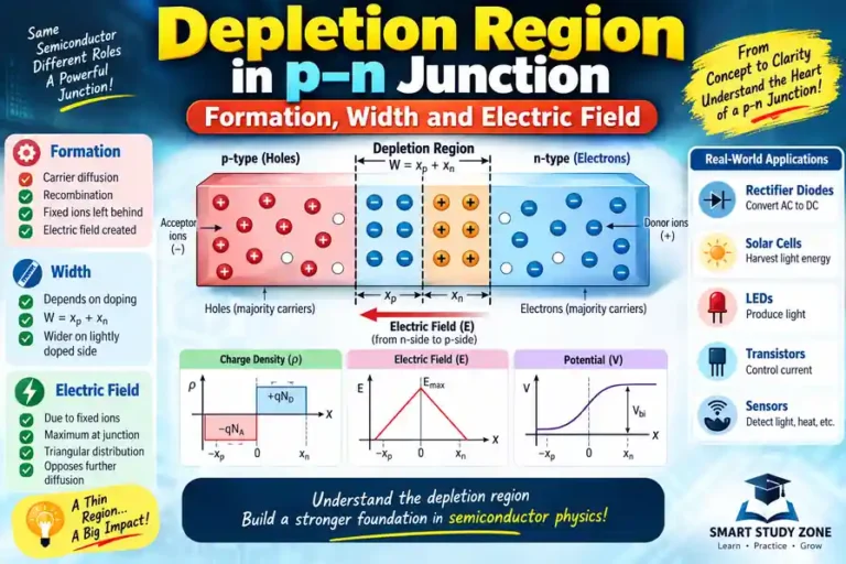
The depletion region in a p–n junction forms naturally when p-type and n-type semiconductors are joined together. As charge carriers move and recombine, they leave behind fixed ions, creating an electric field that acts like an invisible gate controlling carrier motion.
Foundation of Depletion Region in p-n Junction
To understand the depletion region, we must begin with the basic types of semiconductors.
Intrinsic Semiconductor: A pure semiconductor, such as silicon, is called an intrinsic semiconductor.
In such materials:
- Electrons and holes are generated thermally
- Their concentrations are equal
n = p = ni …………………..(1)
where
n = electron concentration
p = hole concentration
ni = intrinsic carrier concentration
Extrinsic Semiconductor: To improve electrical conductivity, semiconductors are doped with impurity atoms.
Two types of doped semiconductors exist.
n-type semiconductor
- Doped with pentavalent atoms
- Majority carriers: electrons
- Minority carriers: holes
Electron concentration is approximately
n ≈ ND ………………………….(2)
Where ND is the donor concentration.
p-type semiconductor
- Doped with trivalent atoms
- Majority carriers: holes
- Minority carriers: electrons
Hole concentration becomes
p ≈ NA ………………………….(3)
where NA represents acceptor concentration.
When these two materials are brought together, the stage is set for p–n junction formation and the emergence of the depletion region.
Depletion Region in p-n Junction
What is the Depletion Region?
The depletion region is the region near the p–n junction where mobile charge carriers are absent due to recombination.
In other words, it is a zone that becomes depleted of free electrons and holes.
Instead of mobile carriers, this region contains:
- Positively charged donor ions on the n-side
- Negatively charged acceptor ions on the p-side
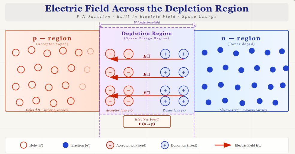
Because these ions are fixed in the crystal lattice, they cannot move. Their presence produces a strong internal electric field across the junction.
Formation of the Depletion Region
The formation of the depletion region begins immediately after a p-type semiconductor is joined with an n-type semiconductor.
Initially:
- The n-region contains a high concentration of electrons.
- The p-region contains many holes.
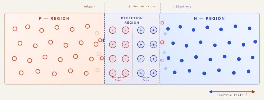
Due to this concentration difference, electrons begin to diffuse from the n-region to the p-region. Similarly, holes diffuse from the p-region to the n-region. When these carriers meet near the junction, they recombine.
As electrons leave the n-region, donor atoms lose their extra electrons and become positively charged ions. Similarly, when holes leave the p-region, acceptor atoms become negatively charged ions.
These fixed ions accumulate near the junction, forming a region devoid of mobile carriers. This region is therefore called the depletion region.
Electric Field in the Depletion Region
The charged ions produce an electric field directed from the n-region toward the p-region.
Due to this electric field, a potential barrier is created, which opposes further diffusion of carriers.
As more carriers diffuse, the electric field grows stronger until it prevents further carrier movement. At this stage:
- Diffusion current equals drift current
- Net current becomes zero
- The junction reaches thermal equilibrium
This equilibrium state defines the stable depletion region in a p–n junction.
Depletion Width
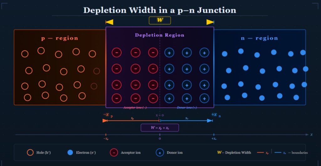
To determine the depletion width mathematically, let us assume xp is the depletion width in the p-region and xn is the depletion width in the n-region. Therefore, the total depletion width is $$W=x_p+x_n\quad……………(4)$$
But according to the charge-neutrality condition, within the depletion region, the total positive charge must equal the total negative charge, since the semiconductor must remain electrically neutral. Hence, $$Q_p=Q_n\quad……………(5)$$
Here, charge on p-side is $$Q_p=qN_A x_p$$
and charge on n-side is $$Q_n=qN_D x_n$$
Therefore, equation (5) becomes $$qN_Ax_p=qN_D x_n$$
$$\Rightarrow x_p=\frac{N_D}{N_A}x_n\quad………………..(6)$$
This equation shows that the depletion region extends more into the lightly doped side.
Now, the electric field inside the depletion region can be obtained using Poisson’s equation
$$\frac{dE}{dx}=\frac{\rho}{\varepsilon_s}$$
where
E = electric field
ρ = charge density
εs = permittivity of semiconductor
Integrating Poisson’s equation across the depletion region gives the electric field distribution. The maximum electric field at the junction is given by
$$E_{max}=\frac{1}{\varepsilon_s}\int_{}^{}\rho dx$$
$$\Longrightarrow E_{max}=\frac{qN_Dx_n}{\varepsilon_s}$$
Similarly, $$E_{max}=\frac{qN_Ax_p}{\varepsilon_s}$$
The built-in potential across the depletion region is obtained by integrating the electric field. $$V_B=\int_{}^{}Edx$$
Carrying out the integration across both regions yields
$$V_B=\frac{qN_Dx_n^2}{2\varepsilon_s}+\frac{qN_Ax_p^2}{2\varepsilon_s}$$
Putting the value of xp from equation (6), the above equation becomes
$$V_B=\frac{qN_D}{2\varepsilon_s}\left( 1+\frac{N_D}{N_A} \right)x_n^2$$
$$\Rightarrow x_n=\sqrt{\frac{2\varepsilon_sV_B}{qN_D\left( 1+\frac{N_D}{N_A} \right)}}\quad………….(7)$$
Using equations (4) and (6), we get,
$$W=x_n\left( 1+\frac{N_D}{N_A} \right)\quad……………..(8)$$
Now using equations (7) and (8), the depletion width becomes
$$W=\sqrt{\frac{2\varepsilon_s}{q}\left( \frac{1}{N_A}+\frac{1}{N_D} \right)V_B}\quad………..(9)$$
This expression reveals several important physical insights:
- The depletion width increases with built-in potential.
• The depletion width decreases when the doping concentration increases.
• The depletion region extends mostly into the lightly doped side.
In practical silicon diodes, the depletion width is typically in the range of
depending on the doping levels.
If one side is heavily doped compared to the other $$N_A>>N_D$$
Then the depletion region extends mostly into the n-side. Thus
$$W\approx x_n$$
and $$W=\sqrt{\frac{q\varepsilon_sV_B}{qN_D}}$$
Thus, by carefully controlling doping levels, engineers can design semiconductor devices with desired electrical characteristics.
Having established the mathematical description of the depletion region, we can now visualize its structure through diagrams.
Interactive p–n Junction Equilibrium Sandbox
Adjust donor ($N_D$) and acceptor ($N_A$) doping to observe the spatial expansion of the depletion width and electric field peak.
⚙️ Depletion Region as a Capacitor
The depletion region contains separated positive and negative charges.
This makes the p–n junction behave somewhat like a capacitor.
A simple depletion-capacitance approximation is
$${C_j=\frac{\varepsilon_sA}{W}}$$
where:
- (Cj) = junction capacitance,
- (A) = junction area,
- (W) = depletion width.
Therefore,
$${C_j\propto\frac{1}{W}}$$
When reverse bias increases, W↑ , so Cj↓
This voltage-dependent capacitance is exploited in varactor diodes and other semiconductor circuits.
Conclusion
The depletion region in a p–n junction is one of the most important concepts in semiconductor physics.
Key takeaways:
- It forms due to carrier diffusion and recombination.
- The region contains fixed ions but no free carriers.
- An internal electric field develops across the region.
- Its width depends on the doping concentration.
- It plays a critical role in the operation of diodes and transistors.
Although microscopic in size, the depletion region governs the behavior of many electronic devices that shape modern technology.
Quick Answer Section | Interview Questions 🎯
# What is the depletion region in a p–n junction?
The depletion region is the region around a p–n junction that contains very few mobile electrons and holes. It forms when electrons and holes diffuse across the junction and recombine. The remaining fixed donor and acceptor ions create a space-charge region and an internal electric field that opposes further majority-carrier diffusion.
# Why is it called the depletion region?
It is called the depletion region because mobile charge carriers are greatly depleted near the junction. Electrons and holes diffuse across the interface and recombine, leaving behind mostly immobile ionized dopant atoms. Therefore, the region has very few mobile majority carriers compared with the neutral p-type and n-type regions.
# What is the direction of the electric field in a p–n junction?
The built-in electric field in an unbiased p–n junction points from the positively charged donor ions on the n-side toward the negatively charged acceptor ions on the p-side. Thus, its conventional direction is from n-side to p-side. This field opposes further majority-carrier diffusion across the junction.
# What happens to the depletion region in forward bias?
In forward bias, the applied electric field opposes the built-in electric field. This reduces the effective potential barrier across the junction, so the depletion region becomes narrower. As a result, majority carriers can cross the junction more easily and the diode current increases rapidly with forward voltage.
# What happens to the depletion region in reverse bias?
In reverse bias, the applied electric field supports the built-in electric field. The potential barrier increases, majority carriers move away from the junction, and the depletion region becomes wider. The wider region also produces a larger junction resistance and generally reduces the depletion capacitance.
# On which side does the depletion region extend more?
The depletion region extends farther into the more lightly doped side. This follows from charge neutrality:
$$N_Ax_p=N_Dx_n$$
If one side has a much smaller doping concentration, a larger distance is required on that side to contain the charge needed to balance the opposite depletion charge.
# What is the formula for depletion width?
For an abrupt p–n junction at equilibrium, the depletion width is
$$W=\sqrt{\frac{2\varepsilon_sV_{B}}{q}\left(\frac{1}{N_A}+\frac{1}{N_D}\right)}$$
The width increases with reverse bias and decreases with forward bias.
# Where is the electric field maximum in a p–n junction?
For an abrupt p–n junction under the depletion approximation, the electric field is maximum at the metallurgical junction. It falls to approximately zero at the depletion-region edges. The maximum field can be expressed as
$$E_{\max}=\frac{2V_{\text{dep}}}{W}$$
# Why does reverse bias increase depletion width?
Reverse bias increases the potential across the depletion region. From
$$W\propto\sqrt{V_{B}+V_R}$$
the depletion width increases with reverse voltage. This wider region contains more uncovered dopant charge and produces a stronger electric field near the junction.
🧮 Solved Numerical Problems
Problem 1: Calculating Depletion Layer Width at Equilibrium
Question: A silicon abrupt p–n junction at room temperature (T = 300 K) has an acceptor concentration NA = 1017 cm-3 and a donor concentration ND = 1016 cm-3. The relative permittivity of silicon is εs = 11.7, and the built-in potential is VB = 0.75 V. Compute the total depletion region width W at zero applied bias.
Solution:
Given:
NA = 1017 cm-3 = 1023 m-3
ND = 1016 cm-3 = 1022 m-3
VB = 0.75 V
εs = 11.7 × 8.854 × 10-12 F/m = 1.036 × 10⁻¹² F/m
q = 1.602 × 10⁻¹⁹ C
Find: Total width W.
Calculation: Using the equilibrium depletion width formula:
$$W = \sqrt{\frac{2 \varepsilon_s V_{B}}{q} \left(\frac{N_A + N_D}{N_A N_D}\right)} $$
Evaluating the bracketed doping factor:
$$\frac{N_A + N_D}{N_A N_D} = \frac{10^{23} + 10^{22}}{10^{23} \times 10^{22}} = \frac{1.1 \times 10^{23}}{10^{45}} $$
$$= 1.1 \times 10^{-22}\text{ m}^3$$
Evaluating the leading coefficient:
$$\frac{2 \varepsilon_s V_{B}} {q} = \frac{2 \times (1.036 \times 10^{-10}\text{ F/m}) \times 0.75\text{ V}}{1.602 \times 10^{-19}\text{ C}} $$
$$= \frac{1.554 \times 10^{-10}}{1.602 \times 10^{-19}} = 9.70 \times 10^8\text{ V}\cdot\text{F/C}$$
Multiplying both terms inside the root:
$$W^2 = (9.70 \times 10^8) \times (1.1 \times 10^{-22}) = 1.067 \times 10^{-13}\text{ m}^2$$
$$W = \sqrt{1.067 \times 10^{-13}} \approx 3.266 \times 10^{-7}\text{ m} = 0.327\text{ }\mu\text{m}$$
Answer: The total depletion width is W ≈ 0.327 μm (or 3.266 × 10⁻⁷ m).
Problem 2: Determination of Peak Electric Field (Emax)
Question: Using the parameters calculated in Problem 1, compute the magnitude of the peak electric field established at the metallurgical interface.
Solution:
Given:
W = 3.266 × 10⁻⁷ m
VB = 0.75 V
To find: Maximum electric field magnitude Emax.
Calculation:
The built-in potential matches the geometric area of the electric field triangle:
$$V_{B} = \frac{1}{2} \vert{}E_{\max}\vert{} W$$
Rearranging to solve for $\vert{}E_{\max}\vert{}$:
$$\vert{}E_{\max}\vert{} = \frac{2 V_{B}}{W} = \frac{2 \times 0.75\text{ V}}{3.266 \times 10^{-7}\text{ m}} $$
$$\vert{}E_{\max}\vert{} = \frac{1.5}{3.266 \times 10^{-7}} \approx 4.593 \times 10^6\text{ V/m}$$
$$= 45.93\text{ kV/cm}$$
Answer: The maximum electric field at the junction interface is Emax ≈ 4.59 × 10⁶ V/m (45.9 kV/cm).
Problem 3: Penetration Depths into the Respective Sides
Question: For the same diode characterized in Problem 1, calculate the exact distance the depletion zone extends into the p-region (xp) and into the n-region (xn).
Solution:
Given:
W ≈ 0.327 μm (or 3.266 × 10⁻⁷ m)
NA = 1017 cm-3 = 1023 m-3
ND = 1016 cm-3 = 1022 m-3
To find: Penetration depths xp and xn.
Calculation: Applying the charge neutrality relations:
$$x_p = W \left(\frac{N_D}{N_A + N_D}\right) = (3.266 \times 10^{-7}) \left(\frac{10^{22}}{1.1 \times 10^{23}}\right)$$
$$= \frac{3.266 \times 10^{-7}}{11} \approx 2.97 \times 10^{-8}\text{ m}$$
$$x_n = W \left(\frac{N_A}{N_A + N_D}\right) = (3.266 \times 10^{-7}) \left(\frac{10^{23}}{1.1 \times 10^{23}}\right) $$
$$= \frac{3.266 \times 10^{-7} \times 10}{11} \approx 2.969 \times 10^{-7}\text{ m}$$
Answer: The space charge layer extends 29.7 nm into the p-side (xp) and 296.9 nm into the n-side (xn). This confirms that over 90% of the depletion region sits inside the more lightly doped n-side.
Problem 4: Depletion Width Under Reverse Bias
Question: If an external reverse-bias voltage of VR = 5 V is applied to the junction described in Problem 1, calculate the new expanded depletion width.
Solution:
Given:
Zero-bias width Wo = 0.3266 μm
VB = 0.75 V
VR = 5 V (Effective barrier potential = VB + VR = 5.75 V)
To find: Reverse-biased width W(VR ).
Calculation: Because depletion width scales with the square root of barrier potential:
$$\frac{W(V_R)}{W_0} = \sqrt{\frac{V_{bi} + V_R}{V_{bi}}}$$
Substituting the voltage terms:
$$\frac{W(V_R)}{W_0} = \sqrt{\frac{0.75 + 5.0}{0.75}} = \sqrt{\frac{5.75}{0.75}} = \sqrt{7.667} \approx 2.769$$
Calculating final width:
$$W(V_R) = 2.769 \times 0.3266\text{ }\mu\text{m} \approx 0.904\text{ }\mu\text{m}$$
Answer: Under an external reverse bias of 5 V, the depletion width expands to approximately 0.904 μm (904 nm).
📚 Quick Formula Sheet
For rapid revision, remember these equations.
Total depletion width:
$$W=x_p+x_n$$
Charge neutrality:
$$N_Ax_p=N_Dx_n$$
Individual widths:
$$
x_p=\frac{N_D}{N_A+N_D}W$$
$$x_n=\frac{N_A}{N_A+N_D}W$$
Built-in potential:
$$V_B=\frac{kT}{q}\ln
\left(\frac{N_AN_D}{n_i^2}\right)$$
Equilibrium depletion width:
$$W=\sqrt{\frac{2\varepsilon_sV_{B}}{q}\left(
\frac1{N_A}+\frac1{N_D}
\right)}$$
Reverse-bias depletion width:
$$
W_R= \sqrt{
\frac{2\varepsilon_s}{q}
\left(\frac1{N_A}+\frac1{N_D}\right)(V_{B}+V_R)}$$
Forward-bias depletion width:
$$W_F=\sqrt{
\frac{2\varepsilon_s}{q}
\left(\frac1{N_A}+\frac1{N_D}\right)(V_{B}-V_F)}$$
Maximum electric field:
$$E_{\max}=\frac{2V_{\text{dep}}}{W}$$
Junction capacitance:
$$C_j=\frac{\varepsilon_sA}{W}$$
📝 Most Expected Questions / PYQs for Exams
Conceptual Questions:
- What is a depletion region in a p–n junction?
- Explain the formation of the depletion region.
- Why does the depletion region contain fixed ions?
- Why is the electric field directed from n-side to p-side?
- Why does the depletion region extend more into the lightly doped side?
- What is the difference between diffusion current and drift current?
- Explain the role of the depletion region in a p–n diode.
- What happens to depletion width under forward bias?
- What happens to depletion width under reverse bias?
- Why is the depletion region important in a photodiode?
Derivation Questions:
- Derive the expression for depletion width of an abrupt p–n junction.
- Derive the expression for the maximum electric field in a depletion region.
- Derive the expression for (xp) and (xn).
- Derive the built-in potential of a p–n junction.
- Derive the depletion width under reverse bias.
- Derive the junction capacitance of a p–n junction.
- Using Poisson’s equation, derive the electric-field distribution in a p–n junction.
FAQs
1. What is the depletion region in a p–n junction?
It is the region near the junction where mobile charge carriers are absent.
2. Why is it called depletion region?
Because it is depleted of free electrons and holes.
3. What charges exist inside the depletion region?
Fixed donor ions and acceptor ions.
4. What determines depletion width?
Doping concentration and built-in potential.
5. Why is the depletion region important?
It controls current flow in semiconductor devices.