
📢 Read the complete guide till the end to master intrinsic semiconductors in just one sitting and strengthen your engineering physics fundamentals.
Contents
Toggle📖 Introduction:
In solid-state physics, semiconductors occupy a special position between conductors and insulators. Among semiconductors, the simplest and most fundamental type is the intrinsic semiconductor.
An intrinsic semiconductor is a pure semiconductor material, free from any intentional impurities. Understanding intrinsic semiconductors is essential because they form the starting point for all semiconductor devices. Before studying doped (extrinsic) semiconductors, it is important to clearly understand how a pure semiconductor behaves.
In this article, you will know:
✅ What an Intrinsic Semiconductor is
✅ Why silicon and germanium are intrinsic semiconductors
✅ How electrical conduction occurs inside a pure semiconductor
✅ How electron-hole pairs are generated
✅ Why temperature affects conductivity
✅ The energy band model of intrinsic semiconductors
✅ Real-life examples and engineering applications
By the end of this chapter, you will have a solid conceptual foundation that will make advanced semiconductor topics much easier to understand.
🧠 Before Understanding Intrinsic Semiconductor...
Before studying an intrinsic semiconductor in detail, it is helpful to recall a few concepts from energy band theory.
If you have already studied the following topics, understanding intrinsic semiconductors will become much easier:
- 🔗 Formation of Energy Bands in Solids
- 🔗 Classification of Solids Based on Electrical Conductivity
- 🔗 Fermi Level in Solids
These concepts explain why electrons require additional energy to move from the valence band to the conduction band.
🔬 What Exactly Is an Intrinsic Semiconductor?
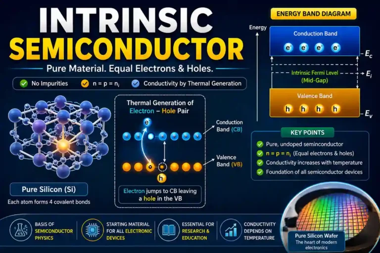
An intrinsic semiconductor is a chemically pure semiconductor material in which no impurity atoms are intentionally added. In other words, it is a semiconductor in its natural and purest form. The most common examples are silicon (Si) and germanium (Ge).
Silicon and germanium atoms each have four valence electrons. Inside the crystal, every atom shares these four electrons with its four nearest neighboring atoms through covalent bonds. This sharing creates a highly ordered and stable three-dimensional arrangement known as the diamond cubic crystal structure. Because all the atoms are identical and uniformly arranged, the crystal exhibits symmetrical electrical and physical properties.
At absolute zero temperature (0 K), every valence electron remains tightly bound in a covalent bond. Since no electron has enough energy to escape from these bonds, no free electrons or holes are available to carry electric current. As a result, a perfectly pure intrinsic semiconductor behaves like an ideal insulator at 0 K. This is an important concept that students often overlook—a true intrinsic semiconductor cannot conduct electricity at absolute zero because it contains no free charge carriers.
When the temperature increases, the crystal lattice absorbs thermal energy, and its atoms begin to vibrate more vigorously. Occasionally, this thermal energy becomes sufficient to break a covalent bond. The bonded electron then gains enough energy to move into the conduction band, where it becomes a free electron capable of carrying electric current.
However, the electron does not leave the crystal without consequence. Its departure creates an empty space in the valence band, known as a hole. Thus, every time one free electron is generated, one hole is created simultaneously. This process is called electron–hole pair generation, and it is the only natural source of charge carriers in an intrinsic semiconductor.
Because electrons and holes are always produced in pairs, their concentrations remain equal in an intrinsic semiconductor. This unique characteristic underpins electrical conduction in pure semiconductor materials and provides the foundation for understanding all semiconductor devices, including p-type and n-type semiconductors, p–n junction diodes, transistors, LEDs, and solar cells.
Hence, in an intrinsic semiconductor:
- There are no impurity atoms.
- Conduction is due to electrons and holes generated by thermal energy.
- The number of electrons is equal to the number of holes.
Mathematically, n=p=ni
where,
- n = electron concentration
- p = hole concentration
- ni = intrinsic carrier concentration
⚛️ Why Silicon and Germanium Are Intrinsic Semiconductors?
At room temperature, the thermal energy available is sufficient to break only a small fraction of these covalent bonds. As a result, a limited number of free electrons and holes are generated naturally. This controlled carrier generation gives silicon and germanium electrical conductivities that lie between those of conductors and insulators.
Another important reason is their moderate energy band gap:
| Material | Approximate Band Gap at 300 K |
|---|---|
| Germanium (Ge) | 0.66 eV |
| Silicon (Si) | 1.12 eV |
A very small band gap would make the material behave almost like a conductor, while a very large band gap would make it an insulator. The moderate band gaps of silicon and germanium enable controlled conduction and make them ideal for electronic devices.
🧱 Crystal Structure of an Intrinsic Semiconductor:
Silicon (Z=14) and germanium (Z=32) belong to Group 14 (IV-A) of the periodic table. Both have four valence electrons in their outermost shell.
To achieve a stable electronic arrangement, each atom shares its four valence electrons with four neighboring atoms. In this way, each atom forms four strong covalent bonds arranged in a tetrahedral pattern, as shown in the following figure. The atoms together form a highly ordered three-dimensional diamond cubic crystal structure.
This regular arrangement gives silicon and germanium the following:
- Strong and stable crystal structures
- Proper sharing of valence electrons
- Very few free charge carriers at low temperature
At very low temperatures, almost all valence electrons remain involved in covalent bonds, so the material has very low electrical conductivity. As the temperature increases, some electrons gain enough thermal energy to break free from their covalent bonds. These electrons become free charge carriers, while the vacancies they leave behind behave as holes.
Thus, the covalent bonding and crystal structure of silicon and germanium provide the foundation for their semiconductor behavior. No impurity is required to create these thermally generated charge carriers in a pure semiconductor.

⚡ Energy Band Structure of an Intrinsic Semiconductor:
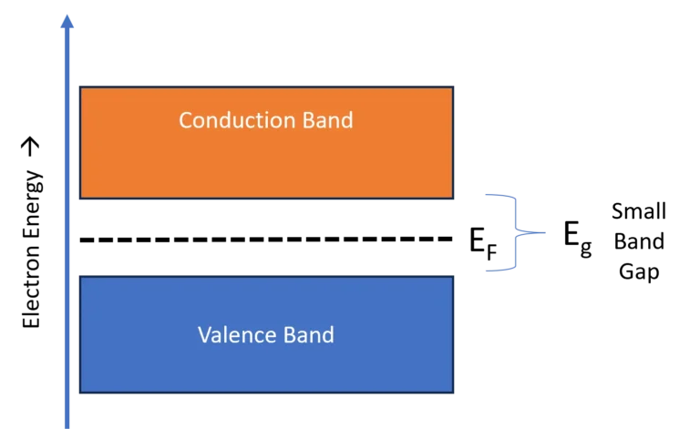
At absolute zero temperature (0 K), a pure semiconductor has a completely filled valence band and a completely empty conduction band. These two bands are separated by a small forbidden energy gap (Eg), as shown in the figure below.
Typical bandgap values are the following:
- Silicon: Eg ≈ 1.1 eV
- Germanium: Eg ≈ 0.66 eV
As the temperature increases, some electrons gain enough thermal energy to cross the energy gap and move from the valence band to the conduction band. When an electron leaves the valence band, it creates an empty position called a hole. Therefore, each excited electron produces one electron–hole pair. Hence, n=p=ni, where ni is the intrinsic carrier concentration.
At thermal equilibrium, electron–hole pairs are continuously generated and recombine, resulting in a definite carrier concentration at a given temperature.
📍 Position of the Fermi Level
In an intrinsic semiconductor, the Fermi level lies approximately midway between the conduction band and valence band.
This means that:
- The electron and hole concentrations are equal.
- The semiconductor has no preferred type of charge carrier.
Thus, the mid-gap position of the Fermi level is an important characteristic of an intrinsic semiconductor.
📈 Intrinsic Carrier Concentration:
The intrinsic carrier concentration is the total number of free electrons (or holes) present per unit volume of a pure semiconductor due to thermal energy.
It is represented by ni. The intrinsic carrier concentration depends on:
- Temperature
- Band gap of the material
With an increase in temperature:
- More covalent bonds break
- More electron–hole pairs are generated
- Conductivity increases
This explains why pure semiconductors show a negative temperature coefficient of resistance.
⚡ Generation of Electron-Hole Pairs:
In an intrinsic semiconductor, all valence electrons participate in covalent bonding at low temperatures. As the temperature increases, some electrons absorb enough thermal energy to overcome the band gap and jump from the valence band to the conduction band.
This process creates two charge carriers simultaneously:
- A free electron in the conduction band
- A hole in the valence band
Since one electron leaves one bond, the number of electrons generated is always equal to the number of holes created.
This phenomenon is known as electron-hole pair generation and forms the basis of electrical conduction in intrinsic semiconductors.
The generation process is continuous. At the same time, free electrons may lose energy and recombine with holes. At thermal equilibrium, the rate of generation equals the rate of recombination, maintaining a constant intrinsic carrier concentration for a given temperature.
⚡ Electrical Conduction in Intrinsic Semiconductor:
When an external electric field is applied:
- Conduction band electrons move toward the positive terminal
- Holes move toward the negative terminal
- Both movements contribute to the electric current
Because the number of charge carriers is limited, intrinsic semiconductors have low conductivity at room temperature compared to metals.
⚡ Electrical Conductivity of an Intrinsic Semiconductor:
The total electrical current in an intrinsic semiconductor under an applied electric field (E) is the sum of two independent drift currents: the drift of free electrons in the conduction band and the drift of holes in the valence band.
The total intrinsic electrical conductivity (σi) is expressed as follows:
Since n = p = ni in a pure semiconductor, we simplify this to:
where:
- μe is the electron mobility (cm2/V . s)
- μh is the hole mobility (cm2/V . s)
📊 Comparison: Intrinsic Semiconductor vs Conductor vs Insulator:
| Feature | Intrinsic Semiconductor | Conductor | Insulator |
|---|---|---|---|
Purity |
Pure semiconductor |
Usually pure metal |
Non-conducting material |
Charge carriers |
Electrons and holes (equal in number) |
Large number of free electrons |
Almost no free charge carriers |
Band gap |
Moderate (≈ 0.5–3 eV) |
Zero or overlapping bands |
Large (> 3 eV) |
Conductivity |
Moderate and temperature-dependent |
Very high |
Extremely low |
Effect of temperature |
Conductivity increases |
Conductivity decreases |
Slight increase only at very high temperatures |
Examples |
Silicon, Germanium |
Copper, Silver, Aluminium |
Glass, Rubber, Mica |
🚀 Applications of Intrinsic Semiconductor:
Although intrinsic semiconductors are rarely used directly in commercial circuits, they form the basis of nearly every semiconductor technology.
1️⃣ Manufacturing of Semiconductor Devices:
High-purity silicon crystals are first prepared as intrinsic semiconductors. Controlled amounts of impurities are then introduced to produce p-type and n-type materials for electronic devices.
Example: Integrated circuits (ICs), transistors, and diodes all begin with intrinsic silicon wafers.
2️⃣ Semiconductor Research Laboratories:
Scientists study intrinsic semiconductors to investigate charge transport, carrier generation, recombination, mobility, and band structure without interference from impurities.
3️⃣ Semiconductor Education:
Intrinsic semiconductors provide the simplest model for understanding semiconductor physics. Concepts such as electron-hole pair generation, Fermi level, and energy bands are first explained using intrinsic materials.
4️⃣ High-Purity Crystal Growth:
The semiconductor industry manufactures extremely pure silicon and germanium crystals before introducing dopants. Maintaining intrinsic purity is essential for fabricating reliable electronic components.
5️⃣ Temperature Sensors:
Because their conductivity varies significantly with temperature, intrinsic semiconductor materials are used in certain temperature-sensitive sensing applications.
🎯 Quick Answer Section:
## What is an intrinsic semiconductor?
An intrinsic semiconductor is a chemically pure semiconductor material without intentionally added impurities. Its electrical conductivity arises from thermally generated electron-hole pairs, and the concentrations of electrons and holes are equal.
## Why are electrons and holes equal in intrinsic semiconductors?
Each electron excited into the conduction band leaves behind one hole in the valence band. Therefore, electrons and holes are always generated in equal numbers.
## Why does conductivity increase with temperature?
Higher temperatures provide more thermal energy to break covalent bonds, generating additional electron-hole pairs and increasing the electrical conductivity.
## Where is the Fermi level in an intrinsic semiconductor?
The intrinsic Fermi level lies approximately at the middle of the forbidden energy gap, indicating equal probabilities for electron and hole populations at thermal equilibrium.
## What is the conductivity equation of an intrinsic semiconductor?
The conductivity is given by:
σ=qni(μn+μp)
where q is the electronic charge, ni is the intrinsic carrier concentration, and μn and μp are the electron and hole mobilities.
## What happens to an intrinsic semiconductor at 0 K?
At absolute zero, every valence electron remains locked in a covalent bond, so no free carriers exist. The material behaves exactly like a perfect insulator with zero conductivity at that temperature.
## Why is electron mobility higher than hole mobility?
Electron mobility (μe) is higher than hole mobility (μh) because electrons move freely through vacant states in the conduction band with lower effective mass, whereas hole conduction involves complex sequential jumping of bound valence electrons between adjacent covalent bonds.
🧮 Solved Numerical Problems:
Question: Determine the total intrinsic electrical conductivity (σi) of Germanium at T = 300 K. Given ni = 2= 2.5 × 1023 cm-3, electron mobility μe = 3800 cm2/V.s, hole mobility μh = 1800 cm2/V.s, and e = 1.6 × 10⁻¹⁹ C.
Solution:
Given:ni = 2= 2.5 × 1023 cm-3, μe = 3800 cm2/V.s, μh = 1800 cm2/V.s, e = 1.6 × 10⁻¹⁹ C
To Find: Intrinsic conductivity σi.
Calculation:
Answer: The intrinsic conductivity of Germanium at 300 K is 0.0224 S/cm.
🎓 PYQs / Most Expected Examination Questions:
Short Answer Questions
- Define an intrinsic semiconductor.
- What is an electron–hole pair?
- Where does the Fermi level lie in a pure semiconductor?
Long Answer Questions
- Explain the energy band structure and conduction mechanism of an intrinsic semiconductor with neat diagrams.
- Describe the electrical properties of a pure semiconductor.
Conceptual Questions
- Why does the conductivity of an intrinsic semiconductor increase with temperature?
- Why are electrons and holes equal in number in an intrinsic semiconductor?
❓ FAQs
1. What is an intrinsic semiconductor?
An intrinsic semiconductor is a pure form of semiconductor material without any added impurities. Its electrical conductivity is solely due to the charge carriers (electrons and holes) generated within the material itself.
2. What are common examples of intrinsic semiconductors?
The most common pure semiconductors are silicon and germanium. These materials are widely used because of their suitable electrical properties.
3. How does conduction occur in an intrinsic semiconductor?
Conduction occurs when thermal energy excites electrons from the valence band to the conduction band, leaving behind holes. Both electrons and holes contribute equally to current flow.
4. What is meant by electron-hole pair?
An electron-hole pair is created when an electron gains enough energy to jump to the conduction band, leaving a vacancy (hole) in the valence band.
5. Why is an intrinsic semiconductor electrically neutral?
It remains electrically neutral because the number of electrons is always equal to the number of holes generated.
6. How does temperature affect intrinsic semiconductors?
As the temperature increases, more electrons gain energy and move to the conduction band, increasing conductivity.
📝 Conclusion:
The 🟨 Intrinsic Semiconductor is the cornerstone of semiconductor physics. Although its electrical conductivity is relatively low, it provides the essential foundation for understanding how charge carriers behave in solid materials.
In a pure semiconductor, electrons and holes are generated in equal numbers through thermal excitation, leading to the unique condition n=p=ni. This balanced carrier population, along with concepts such as the intrinsic Fermi level, energy band structure, and temperature-dependent conductivity, forms the basis of all modern semiconductor devices.
Every advanced topic—including extrinsic semiconductors, p–n junction diodes, transistors, LEDs, solar cells, and integrated circuits—builds directly upon the principles of the intrinsic semiconductor. Therefore, developing a strong understanding of this topic is essential for every engineering student and electronics enthusiast.