
What really happens when p-type and n-type semiconductors meet, and how does this tiny junction control the flow of electric current?
From the formation of the depletion region to the potential barrier and one-way conduction, the p-n junction diode reveals the fascinating physics behind many of the electronic devices we use every day.
Read this complete guide and master the p-n junction diode from the basics to advanced.
By the end of this article, you will be able to:
- Explain what a p-n junction diode is.
- Understand how a p-n junction is formed.
- Describe the formation of the depletion region.
- Understand the origin of the potential barrier.
- Explain equilibrium in a p-n junction.
- Describe the energy band diagram of a p-n junction diode.
Contents
Toggle⚡ Introduction
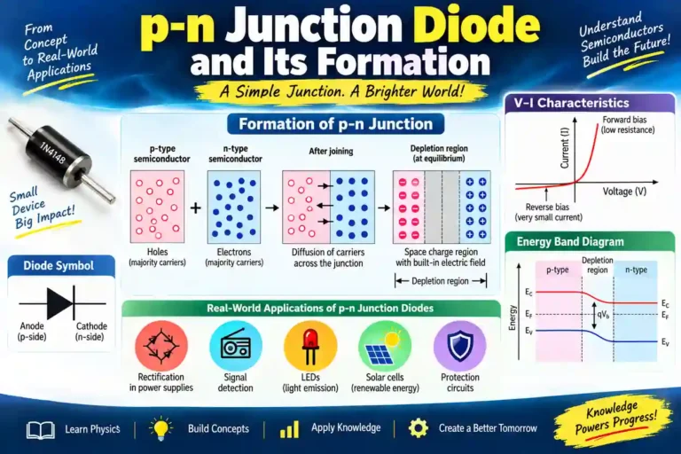
A modern electronic device may look complicated from the outside, but many of its functions begin with a remarkably simple structure: a junction between p-type and n-type semiconductor materials. This junction is called a p-n junction, and when suitable electrical contacts are provided, it forms a p-n junction diode.
A p-n junction diode is one of the most fundamental semiconductor devices because it allows current to flow mainly in one direction. It is formed by joining a p-type semiconductor and an n-type semiconductor within a single crystal. The p–n junction is the basic building block of many electronic devices, such as
- Rectifier diodes
- Transistors
- Solar cells
- Integrated circuits
The behavior of the p–n junction arises from the movement of charge carriers and the establishment of an internal electric field at the junction.
Formation of p–n Junction
The formation of a p–n junction occurs when a p-type semiconductor and an n-type semiconductor are joined together to form a single crystal. This junction creates the basic structure used in semiconductor devices such as diodes and transistors.
Joining of p-type and n-type Materials
To create a p–n junction, different impurities are introduced into different regions of the same semiconductor crystal, i.e.
One region is doped with donor impurities (such as phosphorus or arsenic) to create an n-type region with electrons as majority carriers.
Another region is doped with acceptor impurities (such as boron) to create a p-type region with holes as majority carriers.
This doping is done using techniques such as diffusion or ion implantation.
In this way,
- n-type region has:
- High electron concentration (majority carriers)
- Very few holes (minority carriers)
- p-type region has:
- High hole concentration (majority carriers)
- Very few electrons (minority carriers)
Thus, there exists a carrier concentration gradient across the interface.
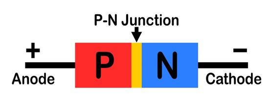
The boundary between the p-type region and the n-type region inside the same crystal is called the p–n junction.
Because both regions belong to the same continuous crystal lattice, the interface is very smooth and electrically stable.
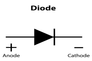
Symbol of a p-n junction diode:
Why the Same Crystal is Used?
When the same semiconductor crystal is used, then:
It ensures good electrical continuity.
It prevents defects at the interface.
It allows proper carrier movement across the junction.
Formation of Depletion Region
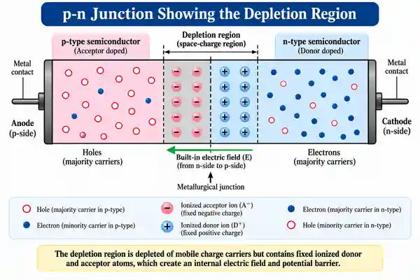
When a p–n junction is formed by joining a p-type semiconductor with an n-type semiconductor, electrons from the n-region diffuse into the p-region, and holes from the p-region diffuse into the n-region due to the difference in carrier concentration.
As these charge carriers diffuse across the junction, they recombine with each other. This leaves behind immobile charged ions near the junction:
- Positive donor ions on the n-side
- Negative acceptor ions on the p-side
The region around the junction where mobile charge carriers are absent is called the depletion region or space charge region.
Why “Depletion”?
Because it is depleted of majority charge carriers (free electrons and holes).
Characteristics:
- Contains immobile ionized donor and acceptor atoms
- Acts like an insulating region
- Creates an internal electric field
The charged ions in the depletion region produce:
An internal electric field
A potential barrier
Eventually, a state of equilibrium is reached in which diffusion and drift currents balance each other.
Why Does the Depletion Region Stop Growing?
The formation of the depletion region produces a separation of fixed charges.
The p-side near the junction contains negatively charged acceptor ions, while the n-side contains positively charged donor ions.
This charge separation produces an electric field inside the depletion region.
The electric field direction is approximately:
$$n\text{-side} \rightarrow p\text{-side} $$
This internal electric field produces a force on mobile charge carriers.
For an electron:
$$\mathbf{F}_n=-q\mathbf{E}$$
For a hole:
$$\mathbf{F}_p=+q\mathbf{E}$$
This field-driven movement is called drift.
Therefore, two opposing processes now exist:
- Diffusion due to carrier concentration gradient
- Drift due to the electric field of the depletion region
As the depletion region becomes wider, the internal electric field becomes stronger.
Eventually, under thermal equilibrium, the diffusion tendency is balanced by the drift tendency.
This is the key physical condition that establishes the equilibrium p-n junction.
Hence, when the junction reaches thermal equilibrium:
$$\text{Diffusion current}=\text{Drift current}$$
Therefore, the net current through the junction is zero.
Built-In Electric Field and Potential Barrier
Internal Electric Field
The separation of positive and negative charges in the depletion region creates an internal electric field directed from the n-side to the p-side.
This electric field opposes the further diffusion of the majority charge carriers.
Potential Barrier
The electric field produces a potential difference across the depletion region of a p–n junction due to the diffusion of electrons and holes after junction formation, called the potential barrier (or built-in potential). This potential barrier prevents additional electrons and holes from diffusing across the junction.
- For silicon, the typical barrier potential ≈ 0.7 V
- For germanium, it is ≈ 0.3 V
After some time:
- Diffusion current (due to concentration gradient)
- Drift current (due to electric field)
become equal and opposite.
At this stage:
- Net current becomes zero
- A junction is said to be in thermal equilibrium
For details about drift and diffusion, click here.
Energy Band Diagram of p–n Junction Diode
The following figure shows the energy band diagram of a p-n junction diode.
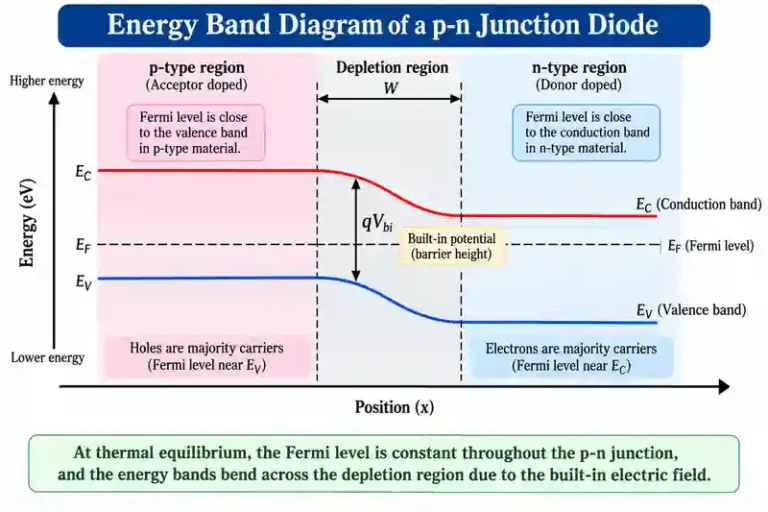
The energy band diagram of a p–n junction diode explains how the conduction band, valence band, and Fermi level behave when a p-type semiconductor is joined with an n-type semiconductor.
Before Joining the p-type and n-type Semiconductors:
Before the junction is formed:
- In the n-type semiconductor, the Fermi level EF lies closer to the bottom of the conduction band EC, because electrons are the majority carriers.
- In the p-type semiconductor, the Fermi level EF lies closer to the top of the valence band EV because holes are the majority carriers.
Thus, the Fermi levels of the two materials are different before contact.
After Forming the p–n Junction (Thermal Equilibrium):
After forming the p-n junction in the energy band diagram, due to the diffusion and recombination process, the conduction band and valence band bend near the junction.
At thermal equilibrium, the Fermi level becomes constant (flat) throughout the entire p–n junction, indicating that no net current flows through the device. The band bending represents the built-in potential barrier formed across the depletion region.
Interactive simulation: watch diffusion build the depletion region until the internal field halts further net carrier flow.
Advantages of a p-n Junction Diode
1. Simple construction: A conventional diode has a relatively simple semiconductor structure.
2. Small size: Semiconductor fabrication allows diodes to be made extremely small.
3. Fast operation: Many semiconductor diodes can respond rapidly to changing electrical signals.
4. Low cost: Diodes are inexpensive and can be manufactured in large quantities.
5. Wide range of applications: The same basic p-n junction principle supports rectification, switching, detection, protection, light emission, and energy conversion.
Limitations of a p-n Junction Diode
Despite its usefulness, a diode has some limitations.
1. Nonlinear behavior: The current does not increase linearly with voltage.
2. Forward voltage drop: A practical diode requires a finite forward voltage before substantial current flows.
3. Reverse leakage current: A small current can flow under reverse bias.
4. Breakdown limitation: Excessive reverse voltage can damage an ordinary diode unless it is designed for breakdown operation.
5. Temperature dependence: Diode characteristics vary with temperature.
These limitations must be considered when selecting a diode for an actual circuit.
Applications of p-n Junction Diodes
The p-n junction is not merely an examination topic. Its behavior appears in many devices that we use every day.
1. Rectification: Diodes convert alternating current into unidirectional or pulsating direct current. This is why diode rectifiers are widely used in power supplies and electronic adapters.
2. Signal Detection: A diode can extract information from certain modulated electrical signals. This principle is used in detector circuits and radio electronics.
3. LED Technology: Light-emitting diodes are semiconductor junction devices in which electron-hole recombination produces light. LEDs are now widely used in displays, indicators, lighting, and communication systems.
4. Solar Cells: A photovoltaic cell uses a semiconductor junction to convert incident light into electrical energy. The p-n junction plays a central role in separating photogenerated charge carriers.
5. Protection Circuits: Diodes can protect electronic components from unwanted voltage spikes and reverse-polarity conditions.
Thus, the p-n junction concept connects directly with several real-world applications introduced at the beginning of this article.
Important Physical Parameters of a p-n Junction
Several quantities are particularly important when analyzing a p-n junction:
- Built-in potential
$$V_B=\frac{kT}{q}\ln
\left(\frac{N_AN_D}{n_i^2}
\right)$$
2. Total depletion width
$$W=\sqrt{\frac{2\varepsilon_s}{q}\left(
\frac{1}{N_A}+\frac{1}{N_D}\right)V_{bi}}$$
3. Charge neutrality
$$N_AW_p=N_DW_n$$
4. Mass-action law
$$np=n_i^2$$
5. Diode equation
$$I=I_0\left[
e^{qV/\eta kT}-1
\right]$$
These equations form a useful mathematical foundation for further study of semiconductor devices.
Quick Answer Section/Interview Question Answer:
# Why does diffusion occur in a p-n junction?
Diffusion occurs because the concentrations of charge carriers are different on the two sides of the junction. Electrons are highly concentrated on the n-side, while holes are highly concentrated on the p-side. Random thermal motion therefore produces a net movement of carriers from regions of higher concentration toward regions of lower concentration.
# What happens to the depletion region under forward bias?
Under forward bias, the external electric field opposes the built-in junction field. Consequently, the depletion region becomes narrower, and the potential barrier decreases. Majority carriers can cross the junction more easily, producing a substantial increase in diode current as the applied voltage increases.
# What happens to a p-n junction under reverse bias?
Under reverse bias, the external electric field supports the built-in electric field. The depletion region therefore becomes wider, and the potential barrier increases. Major carrier diffusion is strongly suppressed, so only a small reverse current normally flows until a sufficiently high reverse voltage causes breakdown.
# What is the difference between drift and diffusion current?
Diffusion current results from a concentration gradient of charge carriers, whereas drift current results from an electric field. In an equilibrium p-n junction, these two current components are equal in magnitude and opposite in direction, giving zero net current through the junction.
PYQs / Most Expected Questions
Short Answer
- What is a p–n junction?
- Define depletion region.
- What is barrier potential?
Long Answer
- Explain the formation of a p–n junction diode with a neat diagram.
- Describe the process of depletion region formation and built-in potential.
Conceptual Questions
- Why does diffusion stop after some time?
- Why does the depletion region act like an insulator?
FAQs
1. What is a PN junction diode?
A PN junction diode is a semiconductor device formed by joining p-type and n-type materials. It allows current to flow easily in one direction while restricting it in the opposite direction.
2. How is a PN junction formed?
A PN junction is formed by combining p-type (hole-rich) and n-type (electron-rich) semiconductor regions in a single crystal, usually of Silicon or Germanium.
3. What happens when p-type and n-type materials are joined?
When they are joined, electrons from the n-side move toward the p-side, and holes from the p-side move toward the n-side. This movement leads to recombination near the junction.
4. What is the depletion region?
The depletion region is the area around the junction where free charge carriers are absent due to recombination. It contains only immobile ions.
5. What is barrier potential (built-in potential)?
Barrier potential is the voltage developed across the depletion region that opposes further movement of charge carriers. It prevents the continuous diffusion of electrons and holes.
6. Why does the depletion region form?
It forms because electrons and holes recombine near the junction, leaving behind charged ions that create an electric field and prevent further carrier movement.
7. What is meant by equilibrium in a PN junction?
Equilibrium is the state where the diffusion of carriers is balanced by the electric field in the depletion region, resulting in no net current flow.
8. What are the types of biasing in a PN junction diode?
There are two types:
- Forward bias
- Reverse bias
9. What is the significance of the depletion region?
The depletion region controls the flow of current and plays a crucial role in the rectifying behavior of the diode.
10. How is a PN junction diode used in real life?
It is used in rectifiers, signal demodulation, voltage regulation, and many electronic circuits.
11. What is the typical barrier potential for silicon and germanium?
- Silicon: approximately 0.7 V
- Germanium: approximately 0.3 V