
Contents
Toggle🚀 Introduction:
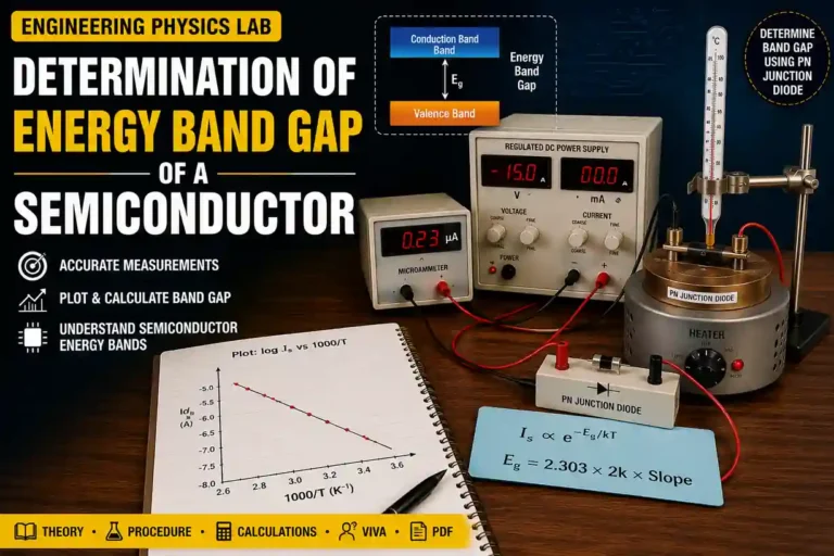
If you’re preparing for your Engineering Physics lab exam, this experiment is one of the most important ones to learn. In this experiment, you will determine the energy band gap of semiconductor, which is a key property that controls its electrical conductivity.
Semiconductors are used in many electronic devices such as smartphones, computers, LEDs, solar cells, and integrated circuits. By performing this experiment, you will understand how the energy band gap is measured and why it plays a vital role in modern electronics. It is also a frequently asked topic in practical exams and viva questions.
🎯 Aim of the Experiment
To determine the energy band gap of a semiconductor.
📝 Importance in Engineering Physics
This experiment is a fundamental part of Engineering Physics laboratories because it connects theoretical concepts such as energy bands, charge carriers, and semiconductor conductivity with practical measurements.
The energy band gap (Eg) is the minimum energy required to excite an electron from the valence band (where electrons are bound to atoms) into the conduction band (where they are free to move and carry a current). By calculating this gap, we determine whether a material will behave as a conductor, an insulator, or a semiconductor.
Understanding band gap energy is essential for the design and operation of diodes, transistors, LEDs, solar cells, and other semiconductor devices.
Students studying this experiment should also understand the concepts of Intrinsic Semiconductor, Extrinsic Semiconductor, Fermi Level, and PN Junction Diode Characteristics, which are closely related topics in semiconductor physics.
🎯 Applications:
Why should you care? Because without managing this band gap, modern technology wouldn’t exist. It is used in:
Designing efficient microprocessors and memory chips.
Developing optoelectronic devices like LEDs, laser diodes, and solar cells.
Creating specialized sensors used in automotive and aerospace engineering.
 Before starting this experiment, read our Intrinsic and Extrinsic Semiconductors guide to understand the basics more easily.
⭐ Experiment Summary:
| Particular | Details |
|---|---|
Aim |
To determine the energy band gap of a semiconductor by measuring the reverse saturation current at different temperatures. |
Apparatus Required |
PN Junction Diode, Regulated DC Power Supply, Microammeter, Voltmeter, Heater, Thermometer, Connecting Wires |
Principle |
The reverse saturation current of a PN junction diode increases with temperature. |
Key Formula |
Is ∝ exp(-Eg/kT) |
Graph |
Plot log Is (Y-axis) against 1000/T (X-axis). The graph is a straight line with a negative slope. |
Observation |
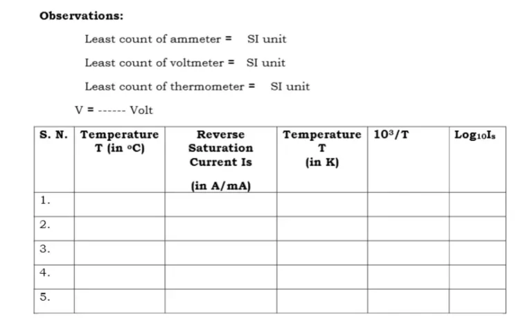
Measure the reverse saturation current (Is) at different temperatures and record the corresponding temperature in Kelvin. |
Calculation |
Calculate the slope of the graph and determine the energy band gap using the standard formula. |
Expected Result |
The energy band gap obtained should be close to the standard value of the semiconductor used (approximately 0.67 eV for Ge or 1.12 eV for Si). |
Applications |
Used in semiconductor devices, transistors, diodes, LEDs, solar cells, integrated circuits, and other electronic components. |
Precautions |
Maintain proper reverse bias, increase temperature gradually, allow thermal equilibrium before taking readings, and avoid loose electrical connections. |
Learning Outcome |
Students learn the concept of energy band gap, temperature dependence of reverse saturation current, graph plotting, and determination of semiconductor properties experimentally. |
📋 Observation Table:
📄Modified Lab Manual PDF:
Below is the complete, high-resolution semiconductor physics lab manual for this experiment.
You can view, download, or print it directly to use during your lab sessions.
📹 Tutorial Video:
💡 Tips for Experimental Accuracy:
To ensure your experimental value matches the standard textbook values (around 0.7 eV for Germanium and 1.1 eV for Silicon), keep these pro-tips in mind:
Avoid Overheating: Never let the thermometer cross 80°C. Overheating can permanently alter the crystalline structure of the semiconductor diode or melt the delicate internal connections.
Take Readings While Cooling: Always record your current values during the cooling cycle rather than the heating cycle. Cooling happens more uniformly, ensuring that the thermometer reading accurately reflects the actual temperature of the internal semiconductor chip.
Watch the Units: Remember to convert Celsius to Kelvin (T = toC + 273) before calculating 1/T or plotting your graph!
💡Exam-Oriented Questions and Answers:
What is the energy band gap of a semiconductor?
The energy band gap is the minimum energy required for an electron to move from the valence band to the conduction band. It determines the electrical conductivity of a semiconductor material.
Why is reverse saturation current used in this experiment?
Reverse saturation current depends strongly on temperature and the semiconductor energy gap. Measuring its variation with temperature helps determine the band gap accurately.
Why does reverse saturation current increase with temperature?
As the temperature increases, more covalent bonds break, generating additional electron-hole pairs. This increases the reverse saturation current significantly.
What is the typical band gap of silicon?
The energy band gap of silicon at room temperature is approximately 1.12 electron volts (eV).
What is the typical band gap of germanium?
The energy band gap of germanium at room temperature is approximately 0.67 electron volts (eV).
Why is a graph plotted between log(Is) and 1/T?
The theoretical relationship becomes linear when expressed in logarithmic form. The slope of the graph is used to calculate the energy band gap.
How does doping affect the band gap of a semiconductor?
Heavy doping introduces allowed energy levels (donor or acceptor levels) inside the forbidden gap, very close to the conduction or valence bands. This effectively reduces the amount of external energy required for carriers to conduct electricity.
Why is the energy band gap of germanium smaller than silicon?
Germanium atoms are larger than silicon atoms, so the outer electrons in Ge are farther from the nucleus and more loosely bound. This weaker binding translates into a smaller energy gap between the valence and conduction bands.
Consequently, Ge becomes conductive at lower temperatures than Si, which also means Ge-based devices have higher leakage currents—a disadvantage that led the electronics industry to favor silicon despite germanium being discovered first.
⚡Viva Questions and Answers:
Q1. What is a semiconductor?
A semiconductor is a material whose conductivity lies between that of conductors and insulators.
Q2. Name two commonly used semiconductors.
Silicon and Germanium.
Q3. What is forbidden energy gap?
It is the energy region between the valence band and conduction band where no electron states exist.
Q4. What is reverse saturation current?
It is the small current flowing through a reverse-biased PN junction due to minority charge carriers.
Q5. Why is reverse bias used in this experiment?
Reverse bias allows measurement of saturation current, which is highly temperature dependent.
Q6. What happens to conductivity when temperature increases?
Conductivity increases because more charge carriers are generated.
Q7. What is the SI unit of energy band gap?
Electron volt (eV) is commonly used.
Q8. What is Boltzmann constant?
It is a physical constant relating thermal energy to temperature.
Q9. Why are semiconductors important?
They are the foundation of modern electronic devices.
Q10. Which semiconductor has a larger band gap: Silicon or Germanium?
Silicon.
Q11. What is the Fermi energy level?
The Fermi level is the highest theoretical energy state that an electron can occupy at absolute zero temperature (0 K). In an intrinsic semiconductor, it lies exactly in the middle of the forbidden energy gap.
Q12. What do you mean by valence band and conduction band?
The valence band is the highest energy band that is fully occupied by electrons at absolute zero temperature. These electrons are bound to their parent atoms. The conduction band is the next higher energy band, which is empty at 0 K. Electrons that acquire sufficient energy (≥ Eg) jump into the conduction band and become free to carry electric current.
❓FAQs:
How is the energy band gap of a semiconductor determined experimentally?
The energy band gap is determined by measuring reverse saturation current at different temperatures and analyzing the graph between log(Is) and reciprocal temperature.
Why does reverse saturation current increase exponentially with temperature?
Higher temperatures generate more electron-hole pairs, resulting in a rapid increase in reverse saturation current.
What is the energy band gap of silicon?
Silicon has an energy band gap of approximately 1.12 eV at room temperature.
What is the difference between silicon and germanium band gaps?
Silicon has a larger band gap (1.12 eV), while germanium has a smaller band gap (0.67 eV).
What are the applications of semiconductor band gap studies?
Band gap studies are useful in the design of solar cells, LEDs, transistors, photodiodes, integrated circuits, and optoelectronic devices.
🔮Related Experiments:
Students should also study the following related Engineering Physics experiments:
- PN Junction Diode Characteristics
- Solar Cell Characteristics
- Photodiode Characteristics
- LED Characteristics
- Hall Effect in Semiconductors
- Determination of Resistivity by Four Probe Method
- Determination of Planck’s Constant Using an LED
- V-I Characteristics of Zener Diode
- Energy Band Diagram of Semiconductor Devices.