
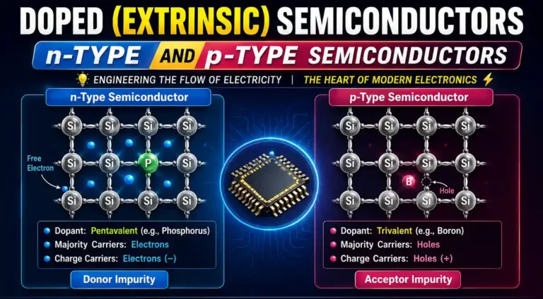
Every diode, transistor, and microchip in your phone owes its existence to one simple trick: deliberately “contaminating” pure silicon with the right impurity atoms. This is doping — and the semiconductors it creates are called extrinsic semiconductors.
Contents
Toggle🔥 Introduction:
An intrinsic semiconductor has very low electrical conductivity at room temperature because the number of charge carriers generated by thermal energy is small. However, for practical electronic applications such as diodes, transistors, and integrated circuits, a much higher and controllable conductivity is required.
This is achieved by adding a very small amount of suitable impurity atoms to a pure semiconductor. This process is known as doping, and the resulting semiconductor is called an extrinsic (doped) semiconductor.
Doping does not destroy the crystal structure of the semiconductor but significantly changes its electrical properties.
By the end of this article, you will be able to:
- Understand the basic mechanism of doping and how pentavalent and trivalent impurities change the concentration and behavior of charge carriers.
- Clearly distinguish between n-type and p-type semiconductors, including their majority and minority carriers.
- Visualize how doping introduces donor and acceptor energy levels and changes the energy-band picture.
- Understand how the Fermi level shifts in n-type and p-type semiconductors after doping.
- Confidently answer common conceptual questions asked in examinations.
📚 What Is a Doped or Extrinsic Semiconductor?
A doped semiconductor is a semiconductor whose electrical properties have been deliberately modified by adding a small and controlled concentration of impurity atoms. The impurity atoms are called dopants.
A pure semiconductor such as silicon or germanium is called an intrinsic semiconductor. When suitable impurities are added to it, it becomes an extrinsic semiconductor.
The purpose of doping is mainly to control the concentration of charge carriers.
🧪Types of Extrinsic Semiconductors:
The type of impurity added to a pure semiconductor determines how its electrical properties change. Based on the valence of the impurity atom, doped semiconductors are broadly classified into two types: n-type and p-type semiconductors.
A suitable dopant can increase the concentration of electrons or holes, making one of them the dominant charge carrier. This difference in the dominant carrier is what distinguishes n-type material from p-type material.
🔵 n-Type Semiconductor:
When a pure tetravalent semiconductor such as silicon (Si) or germanium (Ge) is doped with a small amount of a pentavalent impurity—such as phosphorus (P), arsenic (As), or antimony (Sb)—it becomes an n-type semiconductor.
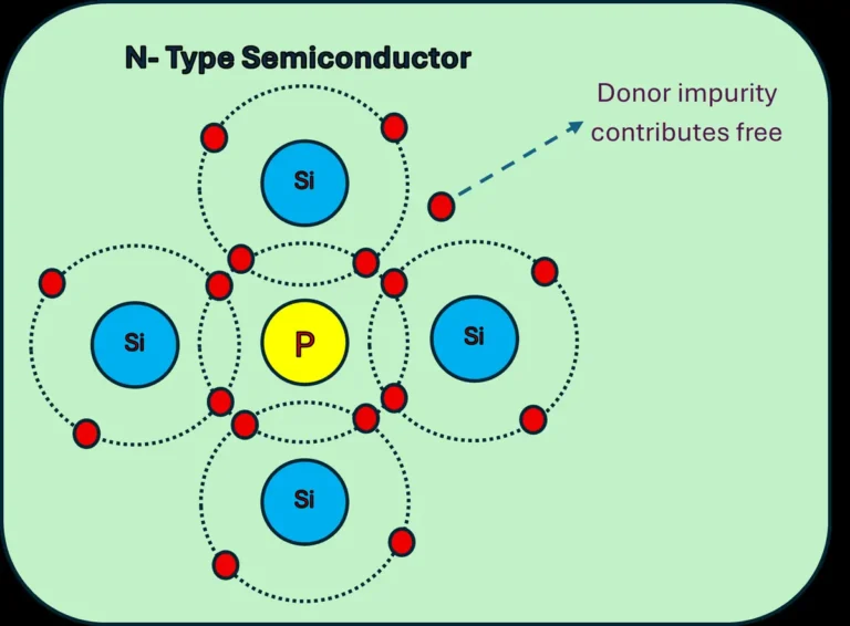
A silicon atom has four valence electrons and normally forms four covalent bonds with its neighboring atoms. When a pentavalent impurity replaces one silicon atom in the crystal lattice, four of its five valence electrons participate in covalent bonding with the surrounding silicon atoms. The fifth electron has no bond to complete, so it remains only weakly bound to the impurity atom. It is shown in Figure 1.
This extra electron requires very little energy to become free. The binding energy is about 0.045 eV in silicon and 0.01 eV in germanium. At room temperature (300 K), thermal energy is approximately 0.026 eV, which is sufficient to release these weakly bound electrons into the conduction band.
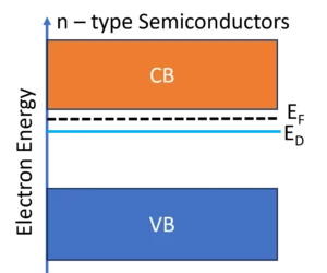
Since the impurity atom contributes an extra electron to the semiconductor, it is called a donor impurity. The energy level introduced by the donor atom just below the conduction band is called the donor energy level, ED, which is slightly below the conduction-band edge EC. Because the energy gap between ED and EC is very small, the donor electron can easily move into the conduction band and participate in electrical conduction.
As a result, the concentration of free electrons becomes much greater than the concentration of holes:
n≫p
Therefore, electrons are the majority carriers, while the relatively few holes produced by thermal generation are the minority carriers.
⚡ Energy Band Diagram of n-Type Semiconductor:
In an n-type semiconductor, the donor energy level lies very close to the conduction band, allowing donor electrons to move easily into the conduction band. As a result of doping, the Fermi level shifts toward the conduction band, indicating an increased electron concentration, as shown in Figure 2.
Consequently, a large number of free electrons become available for electrical conduction, making electrons the majority charge carriers in the material.
🔴 P-Type Semiconductor:
When a pure tetravalent semiconductor such as silicon (Si) or germanium (Ge) is doped with a small amount of a trivalent impurity—such as boron (B), aluminum (Al), gallium (Ga), or indium (In)—it becomes a p-type semiconductor.
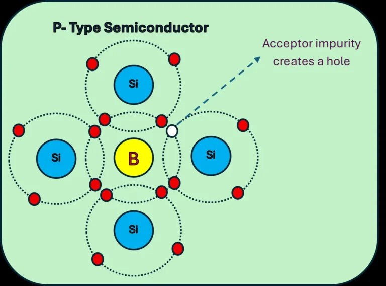
A silicon atom normally uses its four valence electrons to form four covalent bonds with neighboring atoms. However, a trivalent impurity has only three valence electrons, so when it replaces a silicon atom, it can complete only three covalent bonds, as shown in Figure 3.
The fourth bond remains incomplete, creating an electron deficiency known as a hole. An electron from a neighboring covalent bond can easily move into this vacancy, leaving a new hole behind. In this way, the hole effectively moves through the crystal and acts as a positive charge carrier.
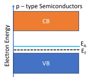
Since the impurity accepts an electron from the surrounding crystal, it is called an acceptor impurity. It introduces an energy level slightly above the valence-band edge, EV, called the acceptor energy level, EA, which allows electrons to move into this level with very little thermal energy.
As a result, the hole concentration becomes much greater than the electron concentration:
p≫n
Thus, holes are the majority carriers, while thermally generated electrons are the minority carriers in a p-type semiconductor.
⚡ Energy Band Diagram of p-Type Semiconductor:
In a p-type semiconductor, the acceptor energy level lies just above the valence band, allowing electrons from the valence band to move easily into the acceptor level and leave behind holes. As a result of doping, the Fermi level shifts toward the valence band, as shown in Figure 4, indicating an increased concentration of holes.
Consequently, a large number of holes become available for electrical conduction, making holes the majority charge carriers in the material.
🔬 n-Type vs p-Type Semiconductor:
| Property | n-Type | p-Type |
|---|---|---|
Impurity |
Pentavalent |
Trivalent |
Example |
P, As, Sb |
B, Al, Ga |
Majority carriers |
Electrons |
Holes |
Minority carriers |
Holes |
Electrons |
Fermi level position |
Near conduction band |
Near valence band |
Conduction due to |
Electrons |
Holes |
📘 Advantages and Limitations of Doping:
Advantages:
Doping offers several important advantages in semiconductor technology. It greatly increases electrical conductivity by increasing the concentration of charge carriers and allows engineers to control both the type and concentration of carriers according to the desired application.
It is also essential for fabricating electronic devices such as diodes, transistors, LEDs, and solar cells. At the same time, when doping is carefully controlled, the impurity atoms can replace a small number of host atoms without significantly disturbing the semiconductor’s crystal structure.
Limitations:
Excessive doping can degrade carrier mobility due to increased impurity scattering, doped semiconductors are more temperature-sensitive at very high doping levels; and achieving extremely uniform doping across a large silicon wafer requires expensive, precise fabrication equipment (like ion implantation or diffusion furnaces).
🏭 Applications of Doped Semiconductors:
Building directly on why doping matters, as introduced above, here’s where n-type and p-type material actually get used:
- PN Junction Diodes: Joining a p-type and an n-type region creates the rectifying junction used in every diode—for full circuit-level behavior, see our lab manual article on the V-I characteristics of PN junction diodes.
- Bipolar Junction Transistors (BJTs): npn and pnp transistors are built from alternating layers of extrinsic semiconductor, forming the amplifying and switching backbone of analog and digital electronics.
- Solar Cells: Photovoltaic cells rely on a p-n junction to separate the electron-hole pairs generated by sunlight, converting light directly into electrical current.
- Integrated Circuits (ICs): Modern microprocessors contain billions of precisely doped n-type and p-type regions arranged as CMOS transistors on a single silicon chip.
- LEDs and Semiconductor Lasers: Recombination of electrons and holes across a doped junction releases energy as light, the working principle behind LEDs and diode lasers.
🔎 Quick Answer Section:
## What is the difference between donor and acceptor impurities?
A donor impurity has an extra valence electron compared with the host semiconductor and can contribute an electron to conduction. An acceptor impurity has one fewer valence electron and can accept an electron, producing a hole. Donors produce n-type material, whereas acceptors produce p-type material.
## How does doping affect the Fermi level?
Doping changes the carrier concentration and therefore shifts the Fermi level. In an n-type semiconductor, the Fermi level moves toward the conduction band because the electron concentration increases. In a p-type semiconductor, it moves toward the valence band because hole concentration increases.
📌 Important Examination Questions:
Short Answer Questions
- What is doping?
- Define donor and acceptor impurities.
- What are majority and minority carriers?
Long Answer / Derivation Questions
- Explain the formation of an n-type semiconductor with a neat energy band diagram.
- Describe a p-type semiconductor and explain its conduction mechanism.
- Compare n-type and p-type semiconductors.
⭐ Very frequently asked in university examinations
Conceptual Questions
- Why does doping increase conductivity so significantly?
- Why is the donor level close to the conduction band?
🎓 Conclusion:
A pure semiconductor provides the foundation, but doping gives engineers control.
By introducing carefully selected impurities into silicon or germanium, we can transform an intrinsic semiconductor into an extrinsic semiconductor with a controlled concentration of charge carriers.
A pentavalent donor impurity contributes an additional electron and produces an n-type semiconductor, in which electrons are the majority carriers.
A trivalent acceptor impurity creates an electron deficiency and produces a p-type semiconductor, in which holes are the majority carriers.
FAQs:
1. What is an extrinsic semiconductor?
An extrinsic semiconductor is a semiconductor material whose electrical conductivity is increased by adding controlled impurities (a process called doping).
2. Why is doping done in semiconductors?
Doping is done to increase the number of charge carriers, thereby improving the conductivity of the semiconductor.
3. What are the types of extrinsic semiconductors?
There are two main types:
- n-type semiconductor
- p-type semiconductor
4. What is an n-type semiconductor?
An n-type semiconductor is formed by adding pentavalent impurities, which provide extra electrons as majority carriers.
5. What is a p-type semiconductor?
A p-type semiconductor is formed by adding trivalent impurities, which create holes as majority carriers.
6. What are common dopants used in semiconductors?
- For n-type: Phosphorus, Arsenic
- For p-type: Boron, Aluminum
7. How does doping affect conductivity?
Doping significantly increases conductivity by introducing more free charge carriers into the semiconductor.
8. What is the role of impurity atoms in extrinsic semiconductors?
Impurity atoms either donate free electrons (donor atoms) or create holes (acceptor atoms), enhancing electrical conduction.
9. What is meant by donor and acceptor impurities?
- Donor impurities provide extra electrons (n-type).
- Acceptor impurities create holes (p-type).
10. How does temperature affect extrinsic semiconductors?
At higher temperatures, intrinsic carrier concentration increases, which can influence the behavior of extrinsic semiconductors.
11. What is the difference between intrinsic and extrinsic semiconductors?
Intrinsic semiconductors are pure, while extrinsic semiconductors are doped to improve conductivity.
12. Why are extrinsic semiconductors widely used in electronics?
Their conductivity can be controlled precisely, making them suitable for devices like diodes, transistors, and integrated circuits.
In doped semiconductors, increasing one type of carrier reduces the other because the product of electron and hole concentrations remains constant
at a given temperature, as required by the law of mass action and the charge neutrality condition.