
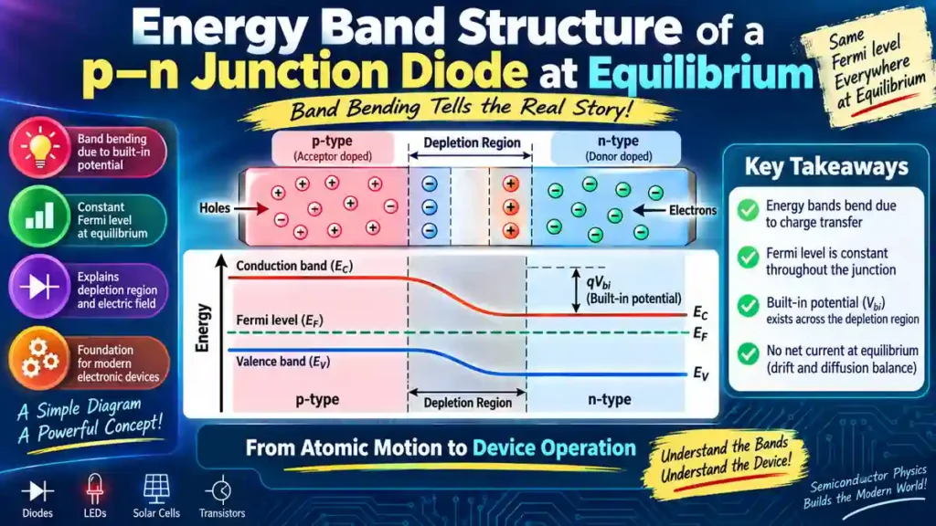
Why do the energy bands bend when a p–n junction reaches equilibrium—and what does that bending actually tell us?
In this article, we’ll uncover the physics behind band bending, the depletion region, built-in potential, and the constant Fermi level—so the equilibrium band diagram becomes something you understand, not something you simply memorize.
Contents
ToggleIntroduction
When we open any modern electronic device like a smartphone, laptop, solar inverter, or medical sensor, we find at the heart of its operation lies a tiny semiconductor junction. This microscopic structure, known as the p–n junction diode, is responsible for controlling the movement of electrical charge.
While the physical junction itself is extremely small, the energy band structure of a p–n junction diode at equilibrium reveals the deeper physics that governs its behavior.
Instead of simply tracking electrons as particles, semiconductor physics often studies their allowed energy levels, known as energy bands. The way these energy bands bend and align at the junction determines the following:
- How current flows
- Why does a potential barrier form?
- Why does the diode conduct only in one direction
In this article, we will explore the energy band structure of a p–n junction diode at equilibrium in a clear, step-by-step manner. By the end, you will know:
- How energy bands behave when p-type and n-type materials join
- Why does the Fermi level become constant at equilibrium
- How the potential barrier forms
- How the band diagram explains diode behavior
Think of this topic as the microscopic blueprint of a diode’s electrical behavior.
Historical Background
The concept of energy bands in solids emerged in the early 20th century as physicists tried to understand why some materials conduct electricity while others do not.
Two developments were particularly important:
Felix Bloch (1928)
Explained how electrons behave in periodic crystal lattices, leading to the concept of energy bands.
Walter Schottky and William Shockley (1930s–1940s)
Applied band theory to semiconductor junctions and helped explain the behavior of p–n junctions and transistors.
Shockley later became one of the inventors of the transistor, which revolutionized electronics.
The energy band diagram of a p–n junction diode became one of the most powerful tools for understanding semiconductor devices.
Energy Bands in Semiconductors
To understand the energy band structure of a p–n junction diode at equilibrium, we must begin with the fundamental concepts of semiconductor band theory.
In a crystalline solid, electrons cannot possess arbitrary energies. Instead, their energies lie in specific allowed ranges called energy bands.
The three most important bands are:
Valence Band (VB)
The highest energy band is filled with electrons at absolute zero.
Conduction Band (CB)
The band where electrons are free to move and contribute to electrical conduction.
Forbidden Energy Gap (Band Gap)
The region between the conduction and valence bands where no electron states exist. $$E_g=E_c-E_v$$
Where
Ec = conduction band bottom energy
Ev = valence band top energy
Eg = band gap energy
For silicon:
Fermi Energy Level
The Fermi level is the energy level at which the probability of electron occupation is 50%.
It indicates the distribution of electrons in energy states.
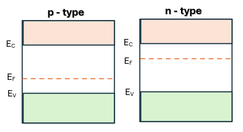
For different materials:
| Material | Fermi Level Position |
|---|---|
Intrinsic semiconductor |
near middle of band gap |
n-type semiconductor |
closer to conduction band |
p-type semiconductor |
closer to valence band |
p-type Semiconductor
In a p-type semiconductor, acceptor impurities (like boron) create holes.
Properties:
Majority carriers → holes
Minority carriers → electrons
The Fermi level shifts toward the valence band.
n-type Semiconductor
In an n-type semiconductor, donor impurities (like phosphorus) provide extra electrons.
Properties:
Majority carriers → electrons
Minority carriers → holes
The Fermi level shifts toward the conduction band.
These different Fermi levels become crucial when a p–n junction forms, because nature forces the system toward equilibrium.
⚡ What Is the Energy Band Structure of a p–n Junction?
To understand how a p–n junction works at equilibrium, we need to look beyond the movement of electrons and holes and examine their energy levels. An energy band diagram gives us a clear picture of what is happening inside the semiconductor, especially near the junction.
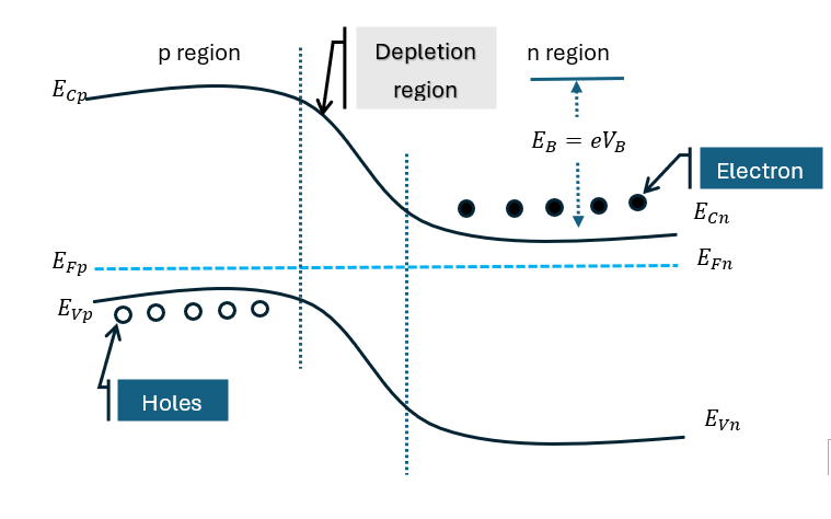
The energy band structure of a p–n junction diode at equilibrium shows how the conduction-band edge (EC), valence-band edge (EV), and Fermi level (EF) change with position from the p-side to the n-side when no external voltage is applied.
Let us understand these three important energy levels one by one.
1. Conduction Band Energy (EC): The conduction band contains energy states in which electrons can move through the semiconductor and contribute to electrical conduction. Its lower boundary is called the conduction-band edge, EC.
Near the p–n junction, EC bends because of the internal electric field.
2. Valence Band Energy (EV): The valence band contains energy states that are normally occupied by electrons. Its upper boundary is called the valence-band edge, EV.
When electrons leave these states, they create holes, which act as positive charge carriers. Like EC, the valence band also bends near the junction.
The band gap is given by
3. Fermi Level (EF): The Fermi level represents the electrochemical potential of the semiconductor. Before joining, the p-type and n-type materials generally have different Fermi levels.
After forming the junction and reaching thermal equilibrium, the Fermi level becomes uniform throughout the structure:
Therefore, in the equilibrium band diagram, EF is drawn as a horizontal line, while EC and EV bend near the depletion region.
Energy band structure of a p–n junction diode at equilibrium
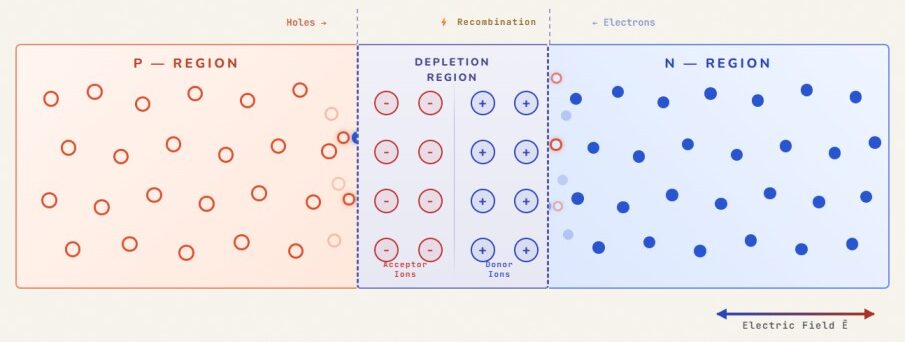
When a p-type semiconductor is joined to an n-type semiconductor, the junction changes. Because the two regions have different carrier concentrations, electrons and holes begin to move across the junction.
Electrons diffuse from the n-side to the p-side, while holes diffuse from the p-side to the n-side. Near the junction, these carriers recombine, leaving behind immobile ionized donor and acceptor atoms. As a result, a depletion region is formed.
The charged ions in this region produce an internal electric field. This field opposes the further diffusion of majority carriers. After a short redistribution of charge, the junction reaches thermal equilibrium, where the drift and diffusion currents exactly balance:
Therefore, although carriers continue to move randomly due to thermal energy, the net current through the junction is zero.
📈 Energy Band Bending at Equilibrium
The depletion region and its electric field directly affect the energy bands.
Before the p-type and n-type materials are joined, their Fermi levels are generally at different positions because their carrier concentrations are different. Once they are connected and reach thermal equilibrium, the Fermi level must become the same throughout the entire structure.
Thus, EF = constant
To establish this common Fermi level, the conduction band EC and valence band EV shift with position near the junction. This change in the band energies is known as band bending.
The complete physical picture can therefore be summarized as
The important point is that band bending is the energy-band representation of the built-in electrostatic potential produced by the depletion region.
At equilibrium, therefore, the p–n junction has a bent conduction band, a bent valence band, and a flat Fermi level, with zero net current as shown in the following figure.
Built-in Potential
The built-in potential is directly related to carrier concentrations. It represents the voltage required to stop the diffusion of majority carriers when the diode is at equilibrium. The built-in potential is given by $$V_B=\frac{kT}{q}ln\left( \frac{N_AN_D}{n_i^2} \right)$$
where k is the Boltzmann constant, T is the temperature, q is the electronic charge, NA and ND are acceptor and donor concentrations, and ni is the intrinsic carrier concentration.
Why Is the Fermi Level Flat at Equilibrium?
A very useful way to remember this is to think of the Fermi level as the level of electrochemical potential.
If the Fermi level varied spatially under true thermal equilibrium, carriers would have a thermodynamic driving force to redistribute.
That would mean the system was not actually at equilibrium.
Therefore:
$$\frac{dE_F}{dx}=0$$
for the ideal equilibrium p–n junction.
Under an applied voltage or other non-equilibrium condition, a single constant Fermi level is generally no longer sufficient to describe the device. Quasi-Fermi levels are then used.
Conclusion
The energy band structure of a p–n junction diode at equilibrium provides a powerful microscopic view of how semiconductor devices operate.
Key points include:
- When p-type and n-type materials join, carrier diffusion begins immediately.
- A depletion region forms, containing immobile ions.
- An internal electric field develops, creating a potential barrier.
- Energy bands bend near the junction to maintain a constant Fermi level.
- The built-in potential determines the electrical behavior of the diode.
Understanding the energy band structure of a p–n junction diode at equilibrium is essential for analyzing semiconductor devices, designing integrated circuits, and advancing modern electronics.
Interactive Band Diagram at Thermal Equilibrium
Quick/Interview Answer Section
# What happens to the energy bands in a p–n junction at equilibrium?
At equilibrium, the conduction and valence bands bend near the junction because of the built-in electric field created by the depletion region. The bands become approximately flat in the neutral regions. The Fermi level remains constant throughout the entire junction.
# Why is the Fermi level constant in a p–n junction at equilibrium?
The Fermi level represents the electrochemical potential. At thermal equilibrium, there can be no net thermodynamic driving force for carrier redistribution. Therefore, the Fermi level becomes uniform throughout the connected p–n junction.
# What causes band bending in a p–n junction?
Band bending is caused by the electrostatic potential created by the fixed ionized donor and acceptor charges in the depletion region. Because electron energy depends on electrostatic potential, the conduction and valence band edges shift through the junction.
# Is there current in a p–n junction at equilibrium?
There is no net current at equilibrium. Electrons and holes still undergo microscopic thermal motion, and diffusion and drift processes can individually occur. However, their corresponding current components cancel, giving Jnet = 0.
# Why do conduction and valence bands bend together?
Both band edges respond to the same electrostatic potential. In a homogeneous semiconductor, their separation remains approximately equal to the band-gap energy (Eg), so the bands shift together as the electrostatic potential changes.
# What is the relation between band bending and electric field?
The spatial slope of the conduction-band energy is related to the electric field by (E=(1/q)(dEC/dx)), with the sign depending on the selected coordinate and energy convention. Therefore, a sloping band indicates an electric field.
PYQs / Most Expected Exam Questions
- Explain the energy band diagram of a p–n junction diode at equilibrium with a neat diagram.
- Derive the expression for the built-in potential of a p–n junction.
- Why is the Fermi level constant in equilibrium?
- Explain the band bending phenomenon in p–n junction.
- Calculate the built-in potential for a silicon diode when doping concentrations are given.
FAQs
1. What is the energy band structure of a p–n junction diode?
It is the graphical representation of the conduction band, valence band, and Fermi level across the junction, showing how energy levels change due to the built-in electric field.
2. Why do energy bands bend in a p–n junction?
Energy bands bend because diffusion of carriers creates an electric field that modifies potential energy across the junction.
3. Why is Fermi level constant at equilibrium?
At thermal equilibrium, no net current flows, so the electrochemical potential (Fermi level) must remain constant.
4. What is built-in potential?
Built-in potential is the internal voltage developed across the depletion region due to charge separation.
5. What happens to the energy band diagram under bias?
Forward bias lowers the barrier, while reverse bias increases it.
I know this web site offers quality depending posts
and additional information, is there any other web page which offers these kinds of information in quality?