When we open any modern electronic device like a smartphone, laptop, solar inverter, or medical sensor, we find at the heart of its operation lies a tiny semiconductor junction. This microscopic structure, known as the p–n junction diode, is responsible for controlling the movement of electrical charge.
Contents
ToggleWhile the physical junction itself is extremely small, the energy band structure of a p–n junction diode at equilibrium reveals the deeper physics that governs its behavior.
Instead of simply tracking electrons as particles, semiconductor physics often studies their allowed energy levels, known as energy bands. The way these energy bands bend and align at the junction determines the following:
- How current flows
- Why does a potential barrier form?
- Why does the diode conduct only in one direction
In this article, we will explore the energy band structure of a p–n junction diode at equilibrium in a clear, step-by-step manner. By the end, you will know:
- How energy bands behave when p-type and n-type materials join
- Why does the Fermi level become constant at equilibrium
- How the potential barrier forms
- How the band diagram explains diode behavior
Think of this topic as the microscopic blueprint of a diode’s electrical behavior.
Historical Background
The concept of energy bands in solids emerged in the early 20th century as physicists tried to understand why some materials conduct electricity while others do not.
Two developments were particularly important:
Felix Bloch (1928)
Explained how electrons behave in periodic crystal lattices, leading to the concept of energy bands.
Walter Schottky and William Shockley (1930s–1940s)
Applied band theory to semiconductor junctions and helped explain the behavior of p–n junctions and transistors.
Shockley later became one of the inventors of the transistor, which revolutionized electronics.
The energy band diagram of a p–n junction diode became one of the most powerful tools for understanding semiconductor devices.
Energy Bands in Semiconductors
To understand the energy band structure of a p–n junction diode at equilibrium, we must begin with the fundamental concepts of semiconductor band theory.
In a crystalline solid, electrons cannot possess arbitrary energies. Instead, their energies lie in specific allowed ranges called energy bands.
The three most important bands are:
Valence Band (VB)
The highest energy band is filled with electrons at absolute zero.
Conduction Band (CB)
The band where electrons are free to move and contribute to electrical conduction.
Forbidden Energy Gap (Band Gap)
The region between the conduction and valence bands where no electron states exist. $$E_g=E_c-E_v$$
Where
Ec = conduction band bottom energy
Ev = valence band top energy
Eg = band gap energy
For silicon:
Fermi Energy Level
The Fermi level is the energy level at which the probability of electron occupation is 50%.
It indicates the distribution of electrons in energy states.
For different materials:
| Material | Fermi Level Position |
|---|---|
|
Intrinsic semiconductor |
near middle of band gap |
|
n-type semiconductor |
closer to conduction band |
|
p-type semiconductor |
closer to valence band |
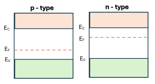
p-type Semiconductor
In a p-type semiconductor, acceptor impurities (like boron) create holes.
Properties:
Majority carriers → holes
Minority carriers → electrons
The Fermi level shifts toward the valence band.
n-type Semiconductor
In an n-type semiconductor, donor impurities (like phosphorus) provide extra electrons.
Properties:
Majority carriers → electrons
Minority carriers → holes
The Fermi level shifts toward the conduction band.
These different Fermi levels become crucial when a p–n junction forms, because nature forces the system toward equilibrium.
Energy Band Structure of a p–n Junction Diode at Equilibrium
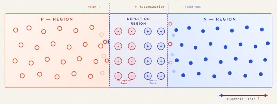
When a p-type semiconductor and an n-type semiconductor are joined, carriers begin to move due to concentration gradients. Electrons diffuse from the n-region to the p-region, and holes diffuse from the p-region to the n-region.
This diffusion leads to recombination near the junction, creating a depletion region.
Inside this region:
- Mobile carriers disappear
- Immobile ions remain
These ions create an internal electric field. Eventually, equilibrium is reached where:
Diffusion current = Drift current.
At this point, no net current flows, and the system is in thermal equilibrium.
Band Bending Phenomenon
Before contact:
- p-region and the n-region have different Fermi levels
After contact:
- Fermi level must become constant
To achieve this, the energy bands bend near the junction.
The conduction band and valence band shift such that the Fermi level EF is constant throughout the entire semiconductor.
This bending represents the built-in electric potential.
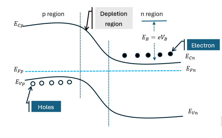
Built-in Potential
The built-in potential is directly related to carrier concentrations. It represents the voltage required to stop the diffusion of majority carriers when the diode is at equilibrium. The built-in potential is given by $$V_B=\frac{kT}{q}ln\left( \frac{N_AN_D}{n_i^2} \right)$$
where k is the Boltzmann constant, T is the temperature, q is the electronic charge, NA and ND are acceptor and donor concentrations, and ni is the intrinsic carrier concentration.
Conclusion
The energy band structure of a p–n junction diode at equilibrium provides a powerful microscopic view of how semiconductor devices operate.
Key points include:
- When p-type and n-type materials join, carrier diffusion begins immediately.
- A depletion region forms, containing immobile ions.
- An internal electric field develops, creating a potential barrier.
- Energy bands bend near the junction to maintain a constant Fermi level.
- The built-in potential determines the electrical behavior of the diode.
Understanding the energy band structure of a p–n junction diode at equilibrium is essential for analyzing semiconductor devices, designing integrated circuits, and advancing modern electronics.
Important Questions (Exam Preparation)
- Explain the energy band diagram of a p–n junction diode at equilibrium with a neat diagram.
- Derive the expression for the built-in potential of a p–n junction.
- Why is the Fermi level constant in equilibrium?
- Explain the band bending phenomenon in p–n junction.
- Calculate the built-in potential for a silicon diode when doping concentrations are given.
FAQs
-
1. What is the energy band structure of a p–n junction diode?
It is the graphical representation of the conduction band, valence band, and Fermi level across the junction, showing how energy levels change due to the built-in electric field.
-
2. Why do energy bands bend in a p–n junction?
Energy bands bend because diffusion of carriers creates an electric field that modifies potential energy across the junction.
-
3. Why is Fermi level constant at equilibrium?
At thermal equilibrium, no net current flows, so the electrochemical potential (Fermi level) must remain constant.
-
4. What is built-in potential?
Built-in potential is the internal voltage developed across the depletion region due to charge separation.
-
5. What happens to the energy band diagram under bias?
Forward bias lowers the barrier, while reverse bias increases it.