
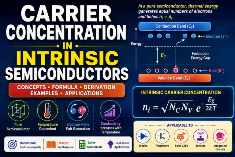
Carrier Concentration in Intrinsic Semiconductors explains how many free electrons and holes are naturally present in a pure semiconductor.
It is a fundamental concept for understanding the electrical behavior of materials such as silicon and germanium.
The carrier concentration strongly depends on temperature, energy band gap, and thermal generation of electron–hole pairs.
Contents
Toggle📚 Introduction:
A pure semiconductor such as silicon or germanium does not have a large number of free charge carriers at very low temperature. However, when its temperature rises above absolute zero, some electrons gain enough thermal energy to move from the valence band to the conduction band. Each electron that leaves the valence band creates a vacancy called a hole.
These electrons and holes become the charge carriers responsible for electrical conduction.
In an intrinsic semiconductor, the number of thermally generated electrons is exactly equal to the number of holes under thermal equilibrium. Therefore,
$$n= p = n_i$$
The quantity (ni), usually called the intrinsic carrier concentration, is one of the most important parameters used to describe semiconductor behavior.
To quantitatively understand semiconductor behavior, we must derive expressions for the following:
- Electron concentration in the conduction band
- Hole concentration in the valence band
- Intrinsic carrier concentration
These derivations are based on:
- Energy band theory
- Density of states
- Fermi–Dirac statistics
By the end of this article, you will be able to derive the expression for intrinsic carrier concentration (ni), explain physically why it depends so sharply on temperature, and solve numerical problems confidently for your exams.
🧮 Carrier Concentration in Intrinsic Semiconductors:
Before deriving the formula, let us understand what the word “carrier concentration” means.
Carrier concentration is the number of mobile charge carriers per unit volume in a semiconductor.
The intrinsic carrier concentration can be obtained by considering the concentrations of electrons in the conduction band and holes in the valence band. Starting with the standard expressions for electron and hole concentrations, we can derive the fundamental relation that connects the intrinsic carrier concentration to the effective density of states, temperature, and the forbidden energy gap.
⚡ Electron Concentration in the Conduction Band:
The electron concentration n represents the number of free electrons present per unit volume in the conduction band. Since an electron can participate in electrical conduction only when it occupies an available state in the conduction band, we need to determine the total number of occupied states.
For this, we consider two important quantities at each energy E:
- Density of states D(E): It tells us how many allowed energy states are available near a particular energy.
- Fermi–Dirac distribution f(E): It gives the probability that an available state at energy E is occupied by an electron.
Therefore, the electron concentration can be understood as
Electron concentration=∫(Density of states)×(Probability of occupation)×dE
To express this mathematically, let dn be the number of electrons per unit volume whose energies lie between E and E+dE. Then,
dn=D(E)f(E)dE ………………..(1)
Here,
- D(E)dE represents the number of available energy states per unit volume within the energy interval E to E+dE.
- f(E) represents the probability that these states are occupied by electrons.
Density of States in the Conduction Band
For a three-dimensional semiconductor, the density of available states in the conduction band is given by:
$$D(E) = \frac{4\pi(2m_e^{*})^{3/2}} {h^{3}}\sqrt{E – E_c}\qquad … (2)$$
where:
- me*= effective mass of electron
- Ec = conduction band minimum energy
- h = Planck’s constant
This tells us how many energy states are available at energy.
Probability of Occupation (Fermi–Dirac Function)
The probability that an energy state at energy E is occupied by an electron is described by the Fermi–Dirac distribution:
$$f(E)=\frac{1}{1 + e^{\frac{(E – E_F)}{kT}}}\qquad … (3) $$
where:
- f(E) = Fermi Function (probability of occupation)
- EF = Fermi energy
- k = Boltzmann’s constant (8.617 × 10⁻⁵ eV/K or 1.38 × 10⁻²³ J/K)
- T = Temperature
For a non-degenerate semiconductor, which is the usual assumption in introductory semiconductor analysis,
$$E-E_F>> 0$$
Therefore, 1 in the denominator becomes negligible compared with the exponential term. The Fermi–Dirac function can then be approximated by the Maxwell–Boltzmann expression:
$$f(E)≈e^{-\left( \frac{E-E_F}{kT} \right)}\qquad … (4)$$
Expression for Electron Concentration
Equation (1) gives the number of electrons within a small energy interval dE. To find the total number of free electrons per unit volume, we must add the contributions from all occupied states throughout the conduction band.
The conduction band begins at EC and extends to the top of the band (∞). Therefore, integrating Eq. (1) over the conduction band gives
$$n = \int_{E_c}^{\infty}D(E)f(E)dE$$
Substituting the values of D(E) and f(E) in the above expressions, we get:
$$n = \int_{E_c}^{\infty}\frac{4\pi(2m_e^{*})^{3/2}} {h^{3}} \sqrt{E – E_c} e^{-(E – E_F)/kT}dE$$
$$n = \int_{E_c}^{\infty}\frac{4\pi(2m_e^{*})^{3/2}} {h^{3}} \sqrt{E – E_c}e^{-(E – E_F + E_c – E_c)/kT}dE$$
$$n = \frac{4\pi(2m_e^{*})^{3/2}} {h^{3}}e^{-(E_c – E_F)/kT}\int_{E_C}^{\infty}{(E – E_C)}^{1/2}e^{-(E – E_C)/kT}dE$$
Let $$\frac{E-E_c}{kT}= x$$ $$=> dE = kT dx $$ Hence, $$n = \frac{4\pi(2m_e^{*})^{3/2}} {h^{3}}e^{-(E_c – E_F)/kT}\int_{0}^{\infty}{(kTx)}^{1/2}e^{-x}kTdx$$
$$n = \frac{4\pi(2m_e^{*}kT)^{3/2}} {h^{3}}e^{-(E_c – E_F)/kT}\int_{0}^{\infty}{(x)}^{1/2}e^{-x}dx$$
Since $$
\int_{0}^{\infty}{x}^{1/2}e^{-x}dx = \left(\frac{\pi}{4}\right)^{1/2}$$
Therefore, $$n = 2\left(\frac{2\pi m_e^{*}kT}{h^{2}} \right)^{3/2}e^{-(E_c – E_F)/kT}$$
$$\color{Red}{\large n = N_c e^{-(E_c – E_F)/kT}\qquad … (5)} $$
This is the formula for electron concentration in the conduction band.
Where $$\mathbf{N_c = 2\left( \frac{2\pi m_e^*kT}{h^2} \right)^{3/2}} \qquad … (6)$$
is called the effective density of states in the conduction band. It is a temperature-dependent constant.
In silicon at 300K, $$N_c = 2.8 \times 10^{25}/m^3$$
🎯 Physical Interpretation:
- Electron concentration increases when:
- Fermi level moves closer to the conduction band
- Temperature increases
- This explains why conductivity increases with temperature
⚡ Hole Concentration in the Valence Band:
The hole concentration (p) is defined as:
The number of holes present in the valence band per unit volume.
A hole represents the absence of an electron.
The number of holes per unit volume in the energy range E and E + dE can be written as
dp = D(E) [1 – f(E)] dE … (7)
Probability of Hole Formation:
The probability of finding a hole in the valence band is the probability that a state is empty, given by 1 – f(E):
$$1 – f(E) = 1 – \frac{1}{1 + e^{\frac{E – E_F}{k_B T}}} = \frac{e^{\frac{E – E_F}{k_B T}}}{1 + e^{\frac{E – E_F}{k_B T}}} $$
For states in the valence band, E – EF << 0; hence, for non-degenerate semiconductors,
$$1-f(E)≈ e^{-(E_F-E)/kT}\qquad … (8)$$
Density of States in the Valence Band
The density of states in the valence band is given by:
$$D(E) = \frac{4\pi(2m_h^{*})^{3/2}} {h^{3}}\sqrt{E_v – E}\qquad … (9)$$
where:
- mh*= effective mass of hole
- Ev = valence band maximum energy
Expression for Hole Concentration
Hence, substituting the values from equations (8) and (9) into equation (7), the number of holes in the energy interval E and E + dE of the valence band is given by
$$dp =\frac{4\pi(2m_h^{*})^{3/2}} {h^{3}}\sqrt{E_v – E}\times e^{-(E_F – E)/kT}$$
The hole concentration in the valence band is obtained by integrating the above equation with a suitable limit. Hence, the hole concentration is given by
$$p = \frac{4\pi(2m_h^{*})^{3/2}} {h^{3}}\int_{-\infty }^{E_v}\sqrt{E_v – E}\times e^{-(E_F – E)/kT}dE$$
$$p = \frac{4\pi(2m_h^{*})^{3/2}} {h^{3}}\int_{-\infty }^{E_v}\sqrt{E_v – E}\times e^{\frac{-(E_F – E + E_v – E_v)} {kT}}dE$$
$$p = \frac{4\pi(2m_h^{*})^{3/2}} {h^{3}} e^{\frac{-(E_F-E_v)} {kT}}\int_{-\infty }^{E_v}\sqrt{E_v – E}\times e^{\frac{(E – E_v)} {kT}}dE$$
Let $$\frac{E_v-E}{kT} = x$$
$$=>dE = -kTdx$$
Substituting values:
$$p = \frac{4\pi(2m_h^{*})^{3/2}} {h^{3}} e^{\frac{-(E_F-E_v)} {kT}}\int_{\infty }^{0}{(kTx)^{1/2} e^{-x}}{(-kTdx)} $$
$$p = \frac{4\pi(2m_h^{*}kT)^{3/2}} {h^{3}} e^{\frac{-(E_F-E_v)} {kT}}\int_{0}^{\infty }{x^{1/2} e^{-x}}{dx}$$
Using the value of integration, we get:
$$p = \frac{4\pi(2m_h^{*}kT)^{3/2}} {h^{3}} e^{\frac{-(E_F-E_v)} {kT}}\left(\frac{\pi}{4} \right)^{1/2}$$
$$p = 2\left( \frac{2\pi m_h^{*}kT}{h^{2}}\right)^{3/2}e^{\frac{-(E_F-E_v)} {kT}} $$
$$\color{Red}{\large p = N_v e^{-(E_F – E_v)/kT}} \qquad … (10) $$
This is the formula for hole concentration in the valence band of intrinsic semiconductors.
Where, $$\mathbf{N_v = 2\left( \frac{2\pi m_h^{*}kT}{h^{2}}\right)^{3/2}} \qquad (11) $$
is the effective density of states in the valence band. For silicon at 300K, $$N_v=10^{25}/m^{3}$$
🎯 Physical Interpretation:
Hole concentration increases when:
- Fermi level moves closer to the valence band
- Temperature increases
📐 Intrinsic Carrier Concentration:
In an intrinsic semiconductor: $$n=p=n_i$$
Multiplying electron and hole concentrations:
$$np=N_cN_v\times e^{-\left( \frac{E_c-E_v}{kT} \right)} $$
But, $$E_c – E_v = E_g$$
Hence: $$np=N_cN_v\times e^{-E_g/kT}$$
$$n_i^{2}=N_cN_v\times e^{-E_g/kT}\qquad (Since, \, np= n_i^2) $$
$$\color{Red}{\large n_i=(N_cN_v)^{1/2}e^{-E_g/2kT}}\qquad … (12) $$
This is the explicit formula for intrinsic carrier concentration.
Since, $$N_c\propto T^{3/2}$$ and
$$N_v\propto T^{3/2}$$
Therefore, $$\mathbf {n_i\propto T^{3/2}e^{-E_g/2kT}} $$
Hence
- Smaller band gap → larger intrinsic carrier concentration
- Higher temperature → rapid increase in carrier concentration
- Germanium has higher carrier concentration than silicon due to a smaller band gap
Substituting the explicit definitions of NC and NV from Eq. (6) and Eq. (11):
❓ Quick Answer Section:
## What is carrier concentration in an intrinsic semiconductor?
Carrier concentration in an intrinsic semiconductor is the number of free electrons or holes present per unit volume of a pure semiconductor at thermal equilibrium. Since every thermally generated electron leaves behind one hole, the electron and hole concentrations are equal. Thus, (n=p=ni), where (ni) represents the intrinsic carrier concentration.
## What is the formula for intrinsic carrier concentration?
The intrinsic carrier concentration is given by
$$
n_i=\sqrt{N_CN_V}\exp\left(-\frac{E_g}{2kT}\right)
$$
where (NC) and (NV) are the effective densities of states, (Eg) is the band-gap energy, (k) is Boltzmann’s constant, and (T) is the absolute temperature.
## Why are electron and hole concentrations equal in an intrinsic semiconductor?
In a pure semiconductor, thermal excitation promotes electrons from the valence band to the conduction band. Every electron that enters the conduction band leaves one vacancy in the valence band. That vacancy behaves as a hole. Therefore, one electron-hole pair is generated at a time, giving (n=p) at equilibrium.
## How does temperature affect intrinsic carrier concentration?
Intrinsic carrier concentration increases strongly with temperature. The relationship is approximately
$$
n_i\propto T^{3/2}e^{-E_g/(2kT)}
$$
As temperature increases, more valence electrons acquire enough thermal energy to cross the forbidden energy gap. Consequently, more electron-hole pairs are generated, and semiconductor conductivity increases.
## What happens to carrier concentration when band gap increases?
At a fixed temperature, intrinsic carrier concentration decreases when the band gap increases because
$$
n_i\propto e^{-E_g/(2kT)}
$$
A larger band gap requires more energy for an electron to reach the conduction band. Therefore, fewer thermally generated electron-hole pairs are produced.
🧮 Solved Numerical Problems:
Problem 1: Calculation of Intrinsic Carrier Concentration:
Question: Calculate the intrinsic carrier concentration of silicon at T = 300 K. Given NC = 2.8 × 1025 m3, NV = 1.04 × 1025 m3, energy bandgap Eg = 1.12 eV, and kB = 8.617 × 10⁻⁵ eV/K.
Solution:
Given: T = 300 K, NC = 2.8 × 1025 m3, NV = 1.04 × 1025 m3, Eg = 1.12 eV, kB T = 8.617 × 10⁻⁵ eV/K × 300 K = 0.02585 eV
To Find: Intrinsic carrier concentration ni.
Calculation: Using Eq. (12):
Answer: The intrinsic carrier concentration of Silicon at 300 K is 2.11 × 10¹⁶ m-3
Problem 2: Temperature Variation Ratio of Carrier Concentration:
Question: Determine the ratio of intrinsic carrier concentration in Silicon at T2 = 400 K compared to T1 = 300 K. Assume Eg = 1.12 eV remains constant and NCNV ∝ T3.
Solution:
Given: T1 = 300 K ⇒ kB T1 = 0.02585 eV,
T2 = 400 K ⇒ kB T2 = 0.03447 eV,
Eg = 1.12 eV
To Find: Ratio ni(400 K) / ni(300 K).
Calculation: Since $$n_i \propto T^{3/2} e^{-E_g / (2 k_B T)}$$
Answer: The intrinsic carrier concentration increases by a factor of approximately 346 when temperature rises from 300 K to 400 K.
Problem 3: Electrical Conductivity of Intrinsic Silicon
Question: Calculate the intrinsic electrical conductivity (σi) of pure Silicon at 300 K. Given ni = 1.5 × 10¹⁶ m-3, electron mobility μe = 0.135 m2 V.s, hole mobility μh = 0.048 m2 V.s, and e = 1.6 × 10⁻¹⁹ C.
Solution:
Given: ni = 1.5 × 10¹⁶ m-3 , μe = 0.135 m2 V.s, μh = 0.048 m2 V.s, e = 1.6 × 10⁻¹⁹ C
To Find: Intrinsic conductivity σi.
Calculation:
Answer: The electrical conductivity of intrinsic Silicon at 300 K is 4.39 × 10⁻⁴ S/m (or Ω-1m-1).
Problem 4: Determine Band-Gap Energy
Question:
At (310,K), a semiconductor has NC = 2.9 × 1019 cm-3, NV = 1.0 × 1019 cm-3, and intrinsic carrier concentration ni = 2.5 × 1011 cm-3. Determine its band-gap energy.
Solution: Using, $$n_i=\sqrt{N_CN_V}e^{-E_g/(2kT)} $$
Rearranging, $$\frac{\sqrt{N_CN_V}}{n_i}=e^{E_g/(2kT)} $$
Taking the natural logarithm,
$$\frac{E_g}{2kT} = ln \frac{\sqrt{N_CN_V}}{n_i}$$
Hence, $$E_g= 2kT\ln\left(\frac{\sqrt{N_CN_V}}{n_i}\right)$$
After substituting the values and solving, we get
$$E_g\approx0.964,eV $$
Therefore, $$ {E_g\approx0.96, eV} $$
🎓PYQs / Most Expected Questions:
Basic Concept Questions
What is intrinsic carrier concentration?
Why are electrons and holes equal in an intrinsic semiconductor?
What is the role of the Fermi level in carrier concentration?
Understanding-Based Questions
Why does electron concentration increase with temperature?
Why is the intrinsic carrier concentration strongly temperature dependent?
What happens to carrier concentration if the band gap increases?
Derivation-Based Questions (Very Important for Exams)
- Derive the expression for electron concentration in the conduction band: $$n=N_ce^{−(E_c−E_F)/kT}$$
- Derive the expression for hole concentration in the valence band: $$p=N_ve^{−(E_F−E_v)/kT}$$
- Derive the expression for intrinsic carrier concentration: $$n_i=(N_cN_v)^{1/2}e^{-E_g/2kT}$$
- Show that: $$np=n_i^2$$
❓ FAQs – People Also Ask:
## Is intrinsic carrier concentration the same for all semiconductors?
No. Intrinsic carrier concentration varies from material to material. It depends strongly on the semiconductor's band-gap energy, effective masses, and temperature. Materials with different band gaps can therefore have very different intrinsic carrier concentrations even when measured at the same temperature.
## What happens to intrinsic carrier concentration at absolute zero?
In the ideal semiconductor model, at 0 K, thermal excitation across the band gap disappears. Therefore, the equilibrium intrinsic carrier concentration approaches zero. As temperature rises above absolute zero, thermally generated carriers appear.
## Does pressure affect carrier concentration?
Indirectly, yes—pressure can slightly change the band gap of a material, which shifts ni exponentially, though this effect is far smaller than the effect of temperature in most everyday conditions.
## How is carrier concentration measured experimentally?
The most common technique is the Hall effect experiment, which measures the Hall voltage to extract carrier concentration and carrier type directly from a current-carrying sample in a magnetic field.
## What is the physical meaning of effective mass (m*) in carrier concentration equations?
Effective mass accounts for the internal periodic potential forces exerted on an electron or hole by the crystal lattice ions. Instead of using the free-electron rest mass (m0), solid-state physics uses m* so that classical Newton's laws can still describe carrier movement inside a quantum crystal lattice.