
Every semiconductor device works because electrons and holes are able to move through the material in a controlled way. But what actually makes these charge carriers move, and how does their motion produce electric current?
In the sections ahead, we’ll explore drift, diffusion, mobility, and carrier current step by step to understand the fascinating physics behind carrier transport in semiconductors.
Contents
Toggle🌟 Introduction
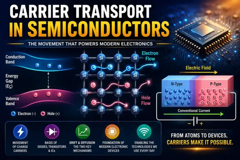
A semiconductor may look like an ordinary piece of solid material, but inside it, something very interesting is happening. Electrons can move through the conduction band, while holes act as positive charge carriers associated with the valence band. When these charge carriers move in a particular direction, they produce an electric current.
The movement of electrons and holes through a semiconductor is known as carrier transport in semiconductors. It is a fundamental concept because it connects carrier motion with important properties such as current, conductivity, mobility, and device performance. The operation of diodes, transistors, solar cells, LEDs, and other semiconductor devices depends on this transport.
But what makes electrons and holes move through a semiconductor? There are two main physical mechanisms responsible for carrier transport:
- An applied electric field causes carriers to move in a preferred direction. This mechanism is called drift.
- A difference in carrier concentration causes carriers to spread from a region of higher concentration toward a region of lower concentration. This mechanism is called diffusion.
Therefore,
This simple expression is the starting point for understanding semiconductor current flow.
These two mechanisms can occur independently, but in many practical semiconductor devices they act at the same time.
Thus, to understand how current flows through a semiconductor, we need to understand both drift and diffusion.
By the end of this article, you’ll be able to derive the drift and diffusion current equations from scratch, connect mobility to the Einstein relation, solve numerical problems confidently, and answer any GATE, JEE, or B.Tech exam question on this topic without memorising a single formula blindly.
⚡ Drift of Charge Carriers
Drift is the transport of charge carriers through a semiconductor under the influence of an external electric field. When an electric field (E) is applied, it exerts an electrostatic force on the mobile charge carriers.
For free electrons, the force is $$F_n = – qE$$
whereas for holes,
$$F_p = + qE$$
Thus, electrons tend to move opposite to the direction of the electric field, while holes move in the same direction as the electric field.
However, carriers do not travel smoothly through the semiconductor. Because of their thermal motion, electrons and holes move randomly and undergo frequent collisions with the atoms, lattice vibrations, and impurities present in the crystal. The applied electric field slightly biases this random motion, giving the carriers a small average velocity in a definite direction. This average velocity is called the drift velocity, denoted by (vd).
For a semiconductor of length (L) and cross-sectional area (A), placed in an electric field of magnitude (E), the magnitude of drift velocity is
For electrons: $$v_{d_{n}}=\mu_nE$$
For holes: $$v_{d_{p}}=\mu_pE$$
where (μn) is the electron mobility and (μp) is the hole mobility.
Mobility therefore tells us how easily a charge carrier responds to an applied electric field. Its SI unit is m2/(Vs).
Once the drift velocity is known, we can determine the drift current produced by the moving charge carriers. Suppose a charge carrier takes time (t) to travel the length (L) of the semiconductor. If (N) charge carriers cross the cross-sectional area (A) during this time, the total charge transported is (qN). Hence, the drift current flowing through the semiconductor is
$$I_d=\frac{qN}{t}=\frac{qNv_d}{L} \qquad \left[ ∵ v_d=\frac{L}{t} \right]$$
This result shows the basic connection between carrier motion and electric current:
Since current density is charge × concentration × velocity, the drift current density is
$$J_d= \frac{I_d}{A}=\frac{qv_dN}{AL}$$
But $$\frac{N}{AL} = n = charge\; carrier\; concentration$$
$$∴\;J_d=nqv_d$$
$$J_d= nq\mu E$$
Hence, electron drift current density $$J_{d_n}= nq\mu_n E$$
and hole drift current density $$J_{d_p}= nq\mu_p E$$
Since both electron and hole drift currents point in the direction of the applied electric field. Therefore, total drift current density is
$$J_{drift}=J_{d_n}+J_{d_p}$$
$$J_{drift}=q\left( n\mu_n+p\mu_p \right) E\qquad … (1)$$
Conductivity of a Semiconductor:
From Ohm’s law in microscopic form,
Comparing this with eq. (1), we obtain $$\sigma=q\left( n\mu_n + p\mu_p \right)\qquad … (2)$$
This is the conductivity of a semiconductor. When doping increases the concentration of mobile carriers, conductivity generally increases—although mobility can decrease at high impurity concentrations because scattering becomes stronger.
🌊 Diffusion of Charge Carriers
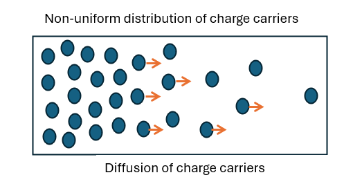
In a semiconductor, electric current can flow even without applying an external electric field. This happens when there exists a concentration gradient of charge carriers.
This type of current is called a diffusion current. Hence, diffusion current is the current produced due to the movement of charge carriers from a region of higher concentration to a region of lower concentration. The charge diffusion is shown in figure (1).
This phenomenon is based on the natural tendency of particles to spread uniformly due to random thermal motion.
Diffusion is especially important in:
- p–n junctions
- Semiconductor devices without external bias
Electron Diffusion Current:
The electron diffusion current density is proportional to the gradient of electron concentration and to the electronic charge, so we may write $$J_{n_{diff}}=qD_n\frac{dn}{dx}$$
Where Dn is the electron diffusion coefficient, which has units of cm²/s and is a positive quantity, and dn/dx is the electron concentration gradient.
If the electron density gradient becomes negative, the electron diffusion current density will be in the negative x direction.
Hole Diffusion Current:
The hole diffusion current density is proportional to the hole density gradient and to the electronic charge, so we may write $$J_{p_{diff}}=-qD_p\frac{dp}{dx}$$
The negative sign appears because:
Holes carry a positive charge.
The direction of the hole motion directly determines the current direction.
Mathematical convention introduces the minus sign.
Where Dp is the hole diffusion coefficient, which has units of cm²/s and is a positive quantity, and dp/dx is the hole concentration gradient.
If the hole density gradient becomes negative, the hole diffusion current density will be in the positive x direction.
Total Diffusion Current:
The total diffusion current density is: $$J_{diff}=J_{n_{diff}}+J_{p_{diff}}$$
$$J_{diff}=qD_n\frac{dn}{dx}-qD_p\frac{dp}{dx}$$
🔄 Total Current Density:
The total current density is the sum of these four components, or, for the one-dimensional case,
$$J=J_{drift}+J_{diff}$$
$$J=q\left( n\mu_n+p\mu_p \right)E+qD_n\frac{dn}{dx}-qD_p\frac{dp}{dx}$$
This equation may be generalized to three dimensions as $$J=q\left( n\mu_n+p\mu_p \right)E+qD_n\nabla n-qD_p\nabla p$$
Electron mobility indicates the efficiency of electron movement in a semiconductor due to the influence of an electric field. The electron diffusion coefficient indicates the efficiency of electron mobility in a semiconductor due to a density gradient.
🔗 Einstein Relation :
Here’s a beautiful question: drift depends on mobility, diffusion depends on the diffusion coefficient—but are these two constants actually related?
Einstein proved that diffusion coefficient and electron mobility are not independent variables. Likewise, the diffusion coefficient and hole mobility are not independent variables.
One of the most important relationships in semiconductor transport connects mobility and diffusion coefficient. It is called the Einstein relation:
$$\frac{D_n}{\mu_n}=\frac{D_p}{\mu_p}=\frac{kT}{q}$$
Here k is Boltzmann’s constant, and the relation kT/q is called the voltage equivalent of temperature. For an electron at T = 300 K, kT/e = 0.026 volts.
📈 Diffusion in p–n Junction:
Diffusion current plays a crucial role in p–n junction formation.
When p-type and n-type materials are joined:
Electrons diffuse from the n to the p side.
Holes diffuse from the p to the n side.
This diffusion creates a depletion region.
A built-in potential develops.
At equilibrium:
Diffusion current = Drift current
Net current = 0
Semiconductor Carrier Transport Simulator
Blue circles = Electrons. Adjust field slider to observe drift; click 'Inject' to see diffusion dispersion.
📊 Comparison: Drift vs Diffusion Current
| Property | Drift Current | Diffusion Current |
|---|---|---|
Cause |
Applied external electric field (E) |
Spatial carrier concentration gradient (∇n, ∇p) |
Carrier Velocity |
Proportional to mobility $$v_d = \mu \mathcal{E}$$ |
Governed by thermal velocity and random scattering |
Governing Law |
Microscopic Ohm’s Law $$J = \sigma \mathcal{E}$$ |
Fick’s First Law of Diffusion $$\Phi = -D \nabla n$$ |
Direction (Electrons) |
Opposite to the E-field vector |
Towards lower concentration regions |
Direction (Holes) |
Along the E-field vector |
Towards lower concentration regions |
Formula (electron) |
$$J_d=nq\mu_nE$$ |
$$J_{diff}=qD_n\frac{dn}{dx}$$ |
Key Parameter |
Carrier Mobility $$\mu_n, \mu_p$$ |
Diffusion Coefficient $$D_n, D_p$$ |
🌡️ Factors Affecting Carrier Transport
Carrier transport does not remain constant under all conditions. Several factors influence the movement of carriers.
- Temperature
As temperature increases, lattice vibrations become stronger. More frequent phonon scattering can reduce mobility.
At the same time, higher temperature can generate more carriers.
Therefore, temperature can affect conductivity through both carrier concentration and mobility.
2. Doping Concentration
Increasing impurity concentration generally increases the number of majority carriers.
However, heavily doped materials can experience stronger impurity scattering, reducing mobility. Mobility is therefore not simply a constant material property.
3. Electric Field
At low electric fields,
So drift velocity increases approximately linearly with electric field.
At sufficiently high fields, however, carrier velocity can approach a saturation region, and the simple low-field mobility model becomes inadequate.
4. Crystal Quality
Defects, vacancies, dislocations, grain boundaries, and interfaces can scatter carriers and reduce transport quality.
⚡ Importance of Carrier Transport Mechanisms
Carrier transport explains the following:
- Electrical conductivity
- p–n junction current
- Diode equation
- Transistor action
- Integrated circuit behaviour
🎯 Quick Answer Section (Viva/Interview Questions)
# What is carrier transport in semiconductors?
Carrier transport in semiconductors is the movement of electrons and holes through a semiconductor. The two principal mechanisms are drift, caused by an electric field, and diffusion, caused by a carrier concentration gradient. Their combined effects determine the current density and are fundamental to the operation of diodes, transistors, solar cells, LEDs, and other semiconductor devices.
# What are the two main mechanisms of carrier transport?
The two main mechanisms are drift and diffusion. Drift occurs when an electric field causes carriers to acquire a net directional velocity. Diffusion occurs when carriers move from regions of higher concentration toward regions of lower concentration. In practical semiconductor devices, both mechanisms can occur simultaneously and contribute to the total current.
# What is drift current in a semiconductor?
Drift current is the current produced when an electric field causes electrons and holes to acquire a net directional velocity. For electrons, the drift current density is Jn = qnμnE, while for holes it is Jp = qnμpE. Both conventional electron and hole current components are directed along the electric field.
# What is diffusion current in a semiconductor?
Diffusion current results from a non-uniform distribution of carriers. Electrons and holes naturally spread from regions of high concentration toward regions of low concentration. The electron diffusion current is Jn = qDndn/dx, while the hole diffusion current is Jp = -qDpdp/dx.
# What is carrier mobility?
Carrier mobility measures how easily an electron or hole responds to an applied electric field. It is defined as the magnitude of the drift velocity divided by the electric field: μ = vd/E. High mobility means that a carrier can acquire a larger drift velocity for the same electric field. Mobility depends on temperature, impurities, defects, and material properties.
# What is the Einstein relation in semiconductors?
The Einstein relation connects carrier mobility with the diffusion coefficient. For a non-degenerate semiconductor near thermal equilibrium, Dn/μn = Dp/μp = kBT/q. It shows that drift and diffusion are related through thermal energy and provides a convenient way to calculate a diffusion coefficient when carrier mobility is known.
# Why is electron mobility higher than hole mobility?
In many common semiconductors such as silicon, electrons have a smaller conductivity effective mass and generally respond more strongly to an electric field than holes. Consequently, electron mobility is typically higher. The exact values depend on temperature, crystal structure, doping, scattering mechanisms, and material composition.
# How does temperature affect carrier transport?
Temperature affects both carrier concentration and mobility. Increasing temperature generally increases lattice vibrations and phonon scattering, which can reduce mobility. However, thermal excitation can also increase the number of carriers. The resulting conductivity therefore depends on which effect dominates in the particular temperature and doping regime.
# What is the drift-diffusion equation?
The drift-diffusion equation describes current produced by both electric-field-driven drift and concentration-gradient-driven diffusion. For electrons, Jn = qnμnE + qDndn/dx, while for holes, Jp = qpμpE – qDpdp/dx. It is a fundamental transport model used in semiconductor device analysis.
# What is thermal voltage in a semiconductor?
Thermal voltage, VT = kT/q, represents the thermal energy per unit charge of carriers. At room temperature (300 K), it equals approximately 0.0259 V and appears in the diode current equation and the Einstein relation.
🔢 Solved Numerical Problems
Problem 1: Drift Current Density Calculation
Question: A uniform silicon bar of cross-sectional area 0.5 cm2 and length 2 cm is doped with Nd = 2 × 1016 cm-3 donor atoms. A voltage of 10 V is applied across its ends. Assuming μn = 1350 cm2/V.s and complete ionization (n = Nd), calculate the drift velocity and drift current density.
Solution:
Given: Length, L = 2 cm,
Applied Voltage, V = 10 V,
Electron Concentration, Nd = 2 × 1016 cm-3
Mobility, μn = 1350 cm2/V.s
Charge, q = 1.6 × 10⁻¹⁹ C
To Find:
- Electric field (E),
- Drift velocity (vdn), and
- Drift current density (Jn(drift)).
Calculation:
Answer:
The drift velocity is 6.75 × 103 cm/s, and the drift current density is 21.6 A/cm2.
Problem 2: Diffusion Current from Linear Gradient
Question: The hole concentration in a slice of germanium varies linearly from p1= 1017 cm-3 at x1 = 0 to p2= 1014 cm-3 at x2 = 0.2 cm. If the hole diffusion constant is Dp= 48 cm2 /s, find the resulting hole diffusion current density.
Solution:
Given:
p1= 1017 cm-3 at x1 = 0
p2= 1014 cm-3 ≈ 0.001 × 1017 cm-3 at x2 = 0.2 cm
Dp= 48 cm2 /s
q = 1.6 × 10⁻¹⁹ C
To Find:
Hole concentration gradient (dp/dx) and
Hole diffusion current density (Jp(diff).
Calculation: Since
Answer:
The hole diffusion current density is +3.84 A/cm2 directed along the +x axis.
Problem 3: Applying the Einstein Relation
Question: An n-type semiconductor at T = 300 K has an electron mobility μn = 850 cm2 /V.s. Calculate the electron diffusion coefficient Dn. (kB= 1.38 × 10⁻²³ J/K, q = 1.6 × 10⁻¹⁹ C).
Solution:
Given: Temperature, T = 300 K
μn = 850 cm2 /V.s
Thermal energy parameter: kB T / q = Vt ≈ 0.02586 V
To Find: Electron diffusion coefficient (Dn).
Calculation: Using the Einstein relation:
Answer: The electron diffusion coefficient is 21.98 cm2/s.
Problem 4: Conductivity and Resistivity of Silicon
Question: An intrinsic silicon sample at 300 K has an intrinsic concentration ni = 1.5 × 1010 cm-3, with electron and hole mobilities of μn = 1400 cm2/V.s and μp = 450 cm2/V.s respectively. Find the intrinsic conductivity and resistivity.
Solution:
Given:
n = p = ni = 1.5 × 1010 cm-3
μn = 1400 cm2/V.s
μp = 450 cm2/V.s
To find: Conductivity (σi) and Resistivity (ρi).
Calculation: Since
Answer: The intrinsic conductivity is 4.44 × 10⁻⁶ S/cm, and the resistivity is 2.25 × 10⁵ Ω.cm.
📝 PYQs / Most Expected Exam Questions
Conceptual Questions
- What is carrier transport in a semiconductor?
- Explain drift and diffusion mechanisms.
- Define carrier mobility and explain its physical significance.
- Why is electron mobility generally greater than hole mobility?
- What factors affect carrier mobility?
- Explain the physical meaning of the diffusion coefficient.
- Distinguish between drift current and diffusion current.
- Why can diffusion occur without an externally applied electric field?
- Explain the significance of the Einstein relation.
- What happens to carrier transport at high electric fields?
Derivation Questions
- Derive the expression for drift velocity.
- Derive the relation
- Derive the electron drift current density.
- Derive the hole drift current density.
- Derive the conductivity of a semiconductor.
- Derive the electron diffusion current equation.
- Derive the hole diffusion current equation.
- Derive the Einstein relation.
- Derive the total drift-diffusion current density.
- Derive the semiconductor continuity equation.
⭐ Very frequently asked in university examinations
❓ FAQs — People Also Ask
## What is the difference between carrier transport and current conduction?
Carrier transport describes the physical movement of electrons and holes inside a semiconductor, while current conduction refers to the resulting flow of electric charge. Transport includes mechanisms such as drift and diffusion. Thus, current is an observable consequence of carrier transport rather than a completely separate phenomenon.
## Does carrier concentration affect mobility?
Yes. Carrier concentration can influence mobility because increasing impurity concentration introduces additional scattering centers. As doping becomes heavier, impurity scattering can become significant and reduce mobility. Therefore, increasing doping may increase conductivity through higher carrier concentration while simultaneously reducing mobility.
## Why is diffusion important in a p–n junction?
Diffusion is essential during the formation of a p–n junction because carriers initially move from their high-concentration regions toward the opposite low-concentration regions. This movement leaves behind charged ionized dopants and contributes to the formation of the depletion region and built-in electric field.
## What is the unit of diffusion coefficient?
The SI unit of the diffusion coefficient is
. In semiconductor engineering, it is frequently expressed in
. The diffusion coefficient describes how rapidly a carrier population spreads because of a concentration gradient.
## What is meant by high-field carrier transport?
High-field transport occurs when the applied electric field becomes sufficiently strong that the simple low-field relation
no longer accurately describes carrier motion. Carrier velocity can approach saturation, and mobility may become field-dependent. More advanced transport models may then be required.