An intrinsic semiconductor has very low electrical conductivity at room temperature because the number of charge carriers generated by thermal energy is small. However, for practical electronic applications such as diodes, transistors, and integrated circuits, a much higher and controllable conductivity is required.
Contents
ToggleThis is achieved by adding a very small amount of suitable impurity atoms to a pure semiconductor. This process is known as doping, and the resulting semiconductor is called an extrinsic (doped) semiconductor.
Doping does not destroy the crystal structure of the semiconductor but significantly changes its electrical properties.
Extrinsic (Doped) Semiconductor
An extrinsic semiconductor is defined as:
A semiconductor whose electrical conductivity is increased by the intentional addition of a small amount of impurity atoms.
Characteristics:
- Impurity concentration is extremely small (about 1 atom per host atom)
- Electrical conductivity increases by several orders of magnitude
- The crystal remains electrically neutral.
Types of Extrinsic Semiconductors
Depending on the type of impurity added, extrinsic semiconductors are classified as follows:
- n-type semiconductors
- p-type semiconductors
n-Type Semiconductor
Formation of n-Type Semiconductor
An n-type semiconductor is formed by doping a pure semiconductor (Si or Ge) with a pentavalent impurity, such as:
- Phosphorus (P)
- Arsenic (As)
- Antimony (Sb)
Pentavalent atoms have five valence electrons.
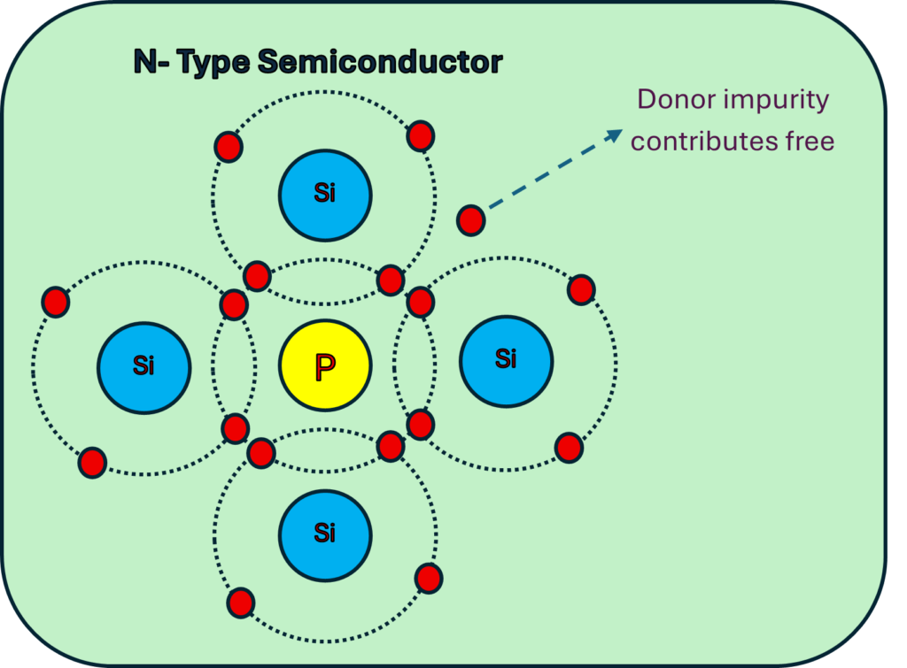
Donor Impurity and Donor Level
When a pentavalent atom replaces a silicon atom in the lattice:
- In an n-type semiconductor, a pentavalent impurity such as phosphorus is added to the silicon crystal.
- The impurity atom forms four covalent bonds with surrounding silicon atoms using four of its five valence electrons.
- The fifth electron remains loosely bound and becomes a free electron, contributing to electrical conduction.
- Thus, electrons are the majority charge carriers in an n-type semiconductor.
- This free electron can be easily excited into the conduction band even at room temperature. The energy level introduced by the donor atom just below the conduction band is called the donor energy level.
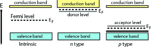
Energy Band Diagram of n-Type Semiconductor
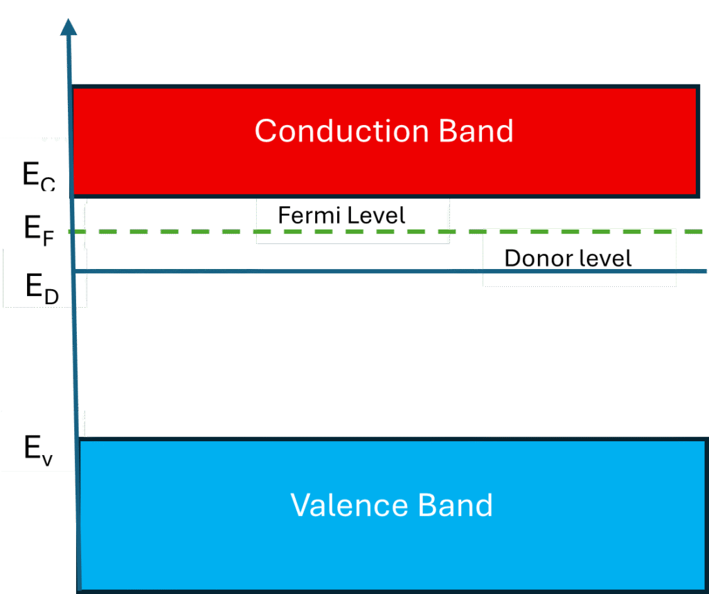
Explanation of Diagram:
- The donor level lies very close to the conduction band
- Fermi level shifts towards the conduction band
- A large number of electrons are available for conduction
Charge Carriers in n-Type Semiconductor
- Majority carriers: Electrons
- Minority carriers: Holes
Electron concentration is much greater than hole concentration:
n >> p
Electrical Conduction
- Conduction occurs mainly due to electrons
- Even a small electric field causes electrons to drift
- Conductivity is much higher than intrinsic semiconductors.
P-Type Semiconductor
Formation of p-type Semiconductor
A p-type semiconductor is formed by doping a pure semiconductor with a trivalent impurity, such as:
- Boron (B)
- Aluminium (Al)
- Gallium (Ga)
Trivalent atoms have three valence electrons.
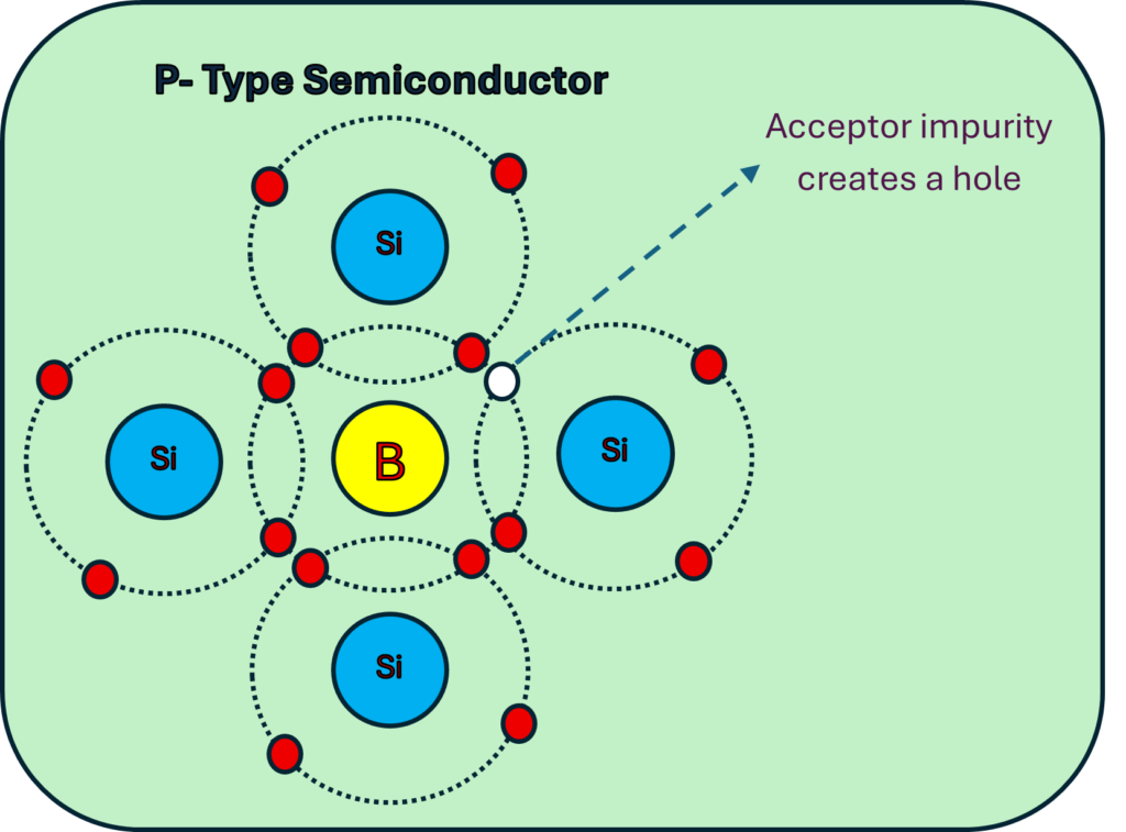
Acceptor Impurity and Acceptor Level
When a trivalent atom replaces a silicon atom:
- In a p-type semiconductor, a trivalent impurity such as boron is introduced into the silicon lattice.
- The impurity atom has only three valence electrons, so it can form only three covalent bonds with silicon atoms.
- One covalent bond remains incomplete, creating an electron deficiency called a hole.
- This hole can move through the lattice as neighbouring electrons fill the vacancy.
- Therefore, holes are the majority charge carriers in a p-type semiconductor.
The energy level introduced just above the valence band is called the acceptor energy level.
Energy Band Diagram of p-Type Semiconductor
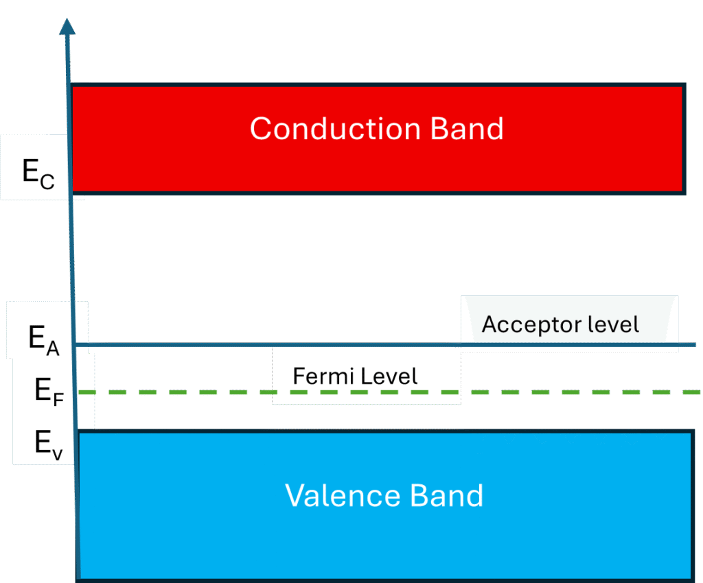
Explanation of Diagram:
- The acceptor level lies just above the valence band
- Fermi level shifts towards the valence band
- A large number of holes are available for conduction
Charge Carriers in p -type Semiconductor
- Majority carriers: Holes
- Minority carriers: Electrons
Hole concentration is much greater than electron concentration:
p >> n
Electrical Conduction
- Conduction occurs mainly due to hole motion
- Holes move toward the negative terminal
- Conductivity is higher than intrinsic semiconductors.
Position of Fermi Level in Extrinsic Semiconductors
- In an n-type, the Fermi level moves closer to the conduction band
- In p-type, the Fermi level moves closer to the valence band
This shift explains the increase in conductivity after doping.
Comparison Between n-Type and p-Type Semiconductors
| Property | n-Type | p-Type |
|---|---|---|
|
Impurity |
Pentavalent |
Trivalent |
|
Example |
P, As, Sb |
B, Al, Ga |
|
Majority carriers |
Electrons |
Holes |
|
Minority carriers |
Holes |
Electrons |
|
Fermi level position |
Near conduction band |
Near valence band |
|
Conduction due to |
Electrons |
Holes |
Advantages of Doping
- Greatly increases conductivity
- Allows control over carrier type and concentration
- Essential for the fabrication of electronic devices
- Maintains crystal structure
Important Examination Questions
Short Answer Questions
- What is doping?
- Define donor and acceptor impurities.
- What are majority and minority carriers?
Long Answer / Derivation Questions
- Explain the formation of an n-type semiconductor with a neat energy band diagram.
- Describe a p-type semiconductor and explain its conduction mechanism.
- Compare n-type and p-type semiconductors.
⭐ Very frequently asked in university examinations
Conceptual Questions
- Why does doping increase conductivity so significantly?
- Why is the donor level close to the conduction band?
FAQs
-
1. What is an extrinsic semiconductor?
An extrinsic semiconductor is a semiconductor material whose electrical conductivity is increased by adding controlled impurities (a process called doping).
-
2. Why is doping done in semiconductors?
Doping is done to increase the number of charge carriers, thereby improving the conductivity of the semiconductor.
-
3. What are the types of extrinsic semiconductors?
There are two main types:
- n-type semiconductor
- p-type semiconductor
-
4. What is an n-type semiconductor?
An n-type semiconductor is formed by adding pentavalent impurities, which provide extra electrons as majority carriers.
-
5. What is a p-type semiconductor?
A p-type semiconductor is formed by adding trivalent impurities, which create holes as majority carriers.
-
6. What are common dopants used in semiconductors?
- For n-type: Phosphorus, Arsenic
- For p-type: Boron, Aluminum
-
7. How does doping affect conductivity?
Doping significantly increases conductivity by introducing more free charge carriers into the semiconductor.
-
8. What is the role of impurity atoms in extrinsic semiconductors?
Impurity atoms either donate free electrons (donor atoms) or create holes (acceptor atoms), enhancing electrical conduction.
-
9. What is meant by donor and acceptor impurities?
- Donor impurities provide extra electrons (n-type).
- Acceptor impurities create holes (p-type).
-
10. How does temperature affect extrinsic semiconductors?
At higher temperatures, intrinsic carrier concentration increases, which can influence the behavior of extrinsic semiconductors.
-
11. What is the difference between intrinsic and extrinsic semiconductors?
Intrinsic semiconductors are pure, while extrinsic semiconductors are doped to improve conductivity.
-
12. Why are extrinsic semiconductors widely used in electronics?
Their conductivity can be controlled precisely, making them suitable for devices like diodes, transistors, and integrated circuits.